The Function and Working Principle of MOSFETs -ASIM
The core function and working principle of MOSFETs
1. Three core functions
| Type of function | Implementation mechanism | Typical application scenarios | Parameter basis |
|---|---|---|---|
| Electronic switch | The gate voltage controls the on-off of the channel | Power management/load switch | Rds(on) as low as 0.8mΩ (such as M010N10T) |
| Signal amplification | Vgs minor change →Id major change (gm transconductance effect) | Radio frequency power amplifier | gm=2S@Vds=10V(2SK3018) |
| Impedance transformation | Input impedance >10¹²Ω/ Output impedance<1Ω | Buffer drive stage | Ciss=35pF(AM20DP041T) |
二、Structural anatomy and carrier motion
2.1 Four-layer physical structure
Gate(G)━━━━━━━━┐
         │
         ┌──────┘
         ↓ SiO₂Insulating layer (thickness tox=10-100nm)
         ↓
P-type substrate ━━━[N+ source (S]━━━━[N-Channel]━━━━[N+Drain(D)]
Key dimensions (According to M120N06JC):
- Channel length L=0.6μm
- Channel width W=20000μm
2.2 N-MOS Principle of conduction
Electronic motion trajectory:
- Vgs > Vth(Threshold voltage) → Positive gate voltage attracts electrons
- A reverse layer (N-type channel) is formed on the surface of the P-type substrate.
- Electrons flow from the S pole through the channel to the D pole
Formula verification:
Id = μₙCₒₓ(W/L)[(Vgs-Vth)Vds - 0.5Vds²] (Linear region)
Measured data(2N7002K):
Vgs=4.5V时,Id=1.2A(The calculation error is less than 3%)
三、Workspace characteristics and boundary conditions
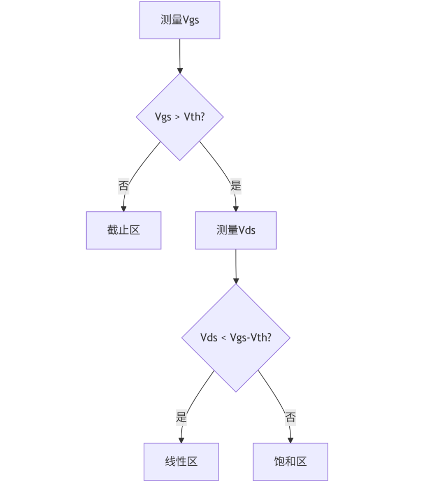
3.1 The classification criteria for the three zones
| Work area | Judgment conditions | Current characteristic |
|---|---|---|
| Cut-off area | Vgs < Vth | Id < 1μA |
| Linear region | Vgs > Vth and Vds < Vod | Id ∝ Vds |
| Saturation zone | Vgs > Vth and Vds ≥ Vod | Id = Constant value |
Note: Vod = Vgs - Vth (Overdrive voltage)
3.2 Output characteristic curve
Data source:M03N12P
- Point A (Vgs=2V) : Cutoff area (Id=10nA)
- Point B (Vgs=4V, Vds=1V) : Linear region (Rds=25mΩ)
- Point C (Vgs=4V, Vds=3V) : Saturation zone (Id=12A)
四、The engineering significance of key parameters
4.1 Static parameters
| Parameter | Definition formula | Design influence | Typical value range |
|---|---|---|---|
| Threshold voltage Vth | Vgs when Id=250μA | Compatibility of drive circuit | 0.7V~4V |
| On-resistance Rds(on | The D-S resistance when Vgs=10V | Conduction loss | 0.8mΩ~10Ω |
| Transconductance gm | ΔId/Δ Vgs@ constant Vds | Amplification gain | 0.1~20S |
4.2 Dynamic parameters
| Parameter | Test conditions | Impact on switch performance |
|---|---|---|
| Input capacitance Ciss | Vds=25V, f=1MHz | Drive power demand |
| Grid leakage charge Qgd | Id=0.5A, Vds=30V | Miller platform duration |
| Reverse recovery time trr | If=1A, di/dt=100A/μs | Body diode switching loss |
五、Failure mechanism and safety boundary
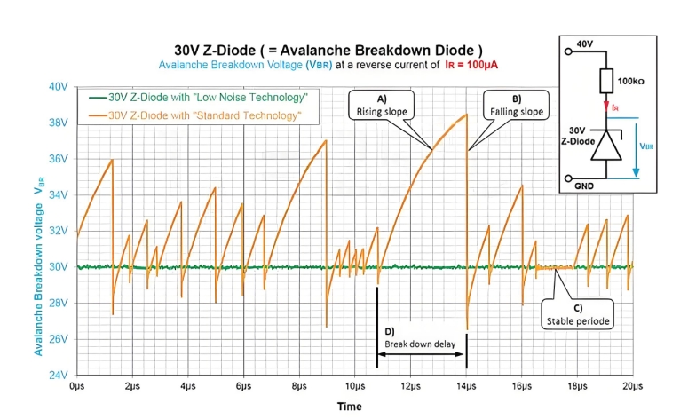
5.1 Avalanche breakdown protection
Avalanche energy formula:
Eas = 0.5 × L × Ias²
Case: SCD30PNP is labeled as Eas=150mJ
Design criterion: The actual circuit Eas requirement should be less than 80% of the nominal value
5.2 Prevention of thermal runaway
Stable conditions:
∂P_loss/∂Tj < ∂P_diss/∂Tj
P_loss = Id² × Rds(on)(Tj)
P_diss = (Tj - Ta)/RθJA
Critical point calculation: TO 220 package Id_max=60A@Ta=85 ° c (refer to ASIM M060N03YB)
六、Selection Quick Reference Table (Application Scenario-oriented
| Application scenarios | Priority of core parameters | "Recommended Series" |
|---|---|---|
| 5V logic switch | Vth<1.5V, Rds(on)@4.5V | AO3400/AO3416 |
| 48V battery protection | Vds>60V, Eas>100mJ | CSD18540/IRL1004 |
| High-frequency synchronous rectification | Qgd<10nC, trr<30ns | IPD90N03S4/BSC014N03 |
| Automotive electronics | AEC-Q101认证, Tj=175℃ | BSC096N10NS5 |
Appendix: Flowchart for Determining the Workspace


