Submit






The ASIM SMA04J24V, SMB06J24V, SMB10J24V, and SMC15J24V share a 24 V VRWM, a 26.7 V to 29.5 V breakdown range, and a 38.9 V maximum VC at their listed pulse-current points. Their IPP values are 10.3 A, 15.5 A, 25.7 A, and 38.6 A.
The shared voltage entries do not make the four parts interchangeable. The numbers are useful only with their stated current, waveform, initial temperature, and package conditions. A selection begins with the real electrical window and ends with board-level verification.
Check the four operating points before discussing package size
| Part number | Package | Peak pulse power class | VRWM | VBR range | IPP | Maximum VC | VC×IPP |
|---|---|---|---|---|---|---|---|
| SMA04J24V | SMA/DO-214AC | 400 W | 24 V | 26.7–29.5 V | 10.3 A | 38.9 V | 400.7 W |
| SMB06J24V | SMB/DO-214AA | 600 W | 24 V | 26.7–29.5 V | 15.5 A | 38.9 V | 603.0 W |
| SMB10J24V | SMB/DO-214AA | 1000 W | 24 V | 26.7–29.5 V | 25.7 A | 38.9 V | 999.7 W |
| SMC15J24V | SMC/DO-214AB | 1500 W | 24 V | 26.7–29.5 V | 38.6 A | 38.9 V | 1501.5 W |
Multiplying maximum VC by the corresponding IPP gives 400.7 W, 603.0 W, 999.7 W, and 1501.5 W. These calculations are arithmetic consistency checks for the listed pulse operating points. They are not additional test results, and they do not turn a peak pulse power rating into continuous dissipation capability. The applicable data sheet still defines the pulse waveform, initial temperature, and repetition limits.
How should the comparison be read?
Start with normal operating voltage and the allowed fault condition. Then compare the maximum clamp voltage or impedance at the relevant test point. Check the package, return path, and channel structure before treating either part as a candidate. This sequence prevents a common error: choosing a device for one excellent number while ignoring the condition that made the number possible.
What changes on a real PCB?
Pads, traces, vias, cable position, and return inductance all change the result at the protected pin. A low-capacitance part on a long branch can still load a high-speed channel. A low clamp rating can still leave the IC with excess voltage if the return path is long. Use the real layout and measure both device terminals and the downstream node when margin is limited.
A practical verification sequence
Freeze sample, load, cable, and operating mode.
Test one part or one layout change at a time.
Record waveforms, current path, function, leakage, and reset or error status.
Restore the original configuration and repeat the test to confirm the change caused the result.
Common questions
Is the part with the lower published value always better?
No. Values must be compared at the same condition and against the actual system requirement.
Can package style decide the selection?
No. Package affects parasitics and assembly, but voltage window, clamp behavior, topology, and layout must also fit.
Why can a catalog-matched device fail in a product?
The full current path includes the enclosure, connector, cable, PCB, and protected circuit. Board-level validation is required.
What the 24 V package comparison actually tells you
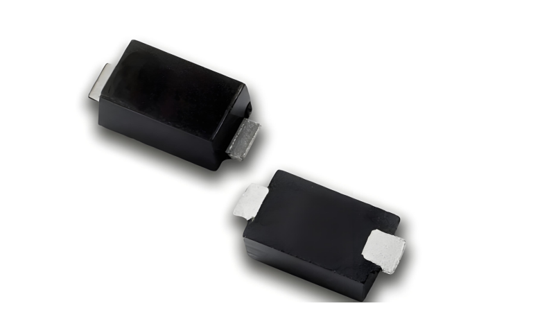
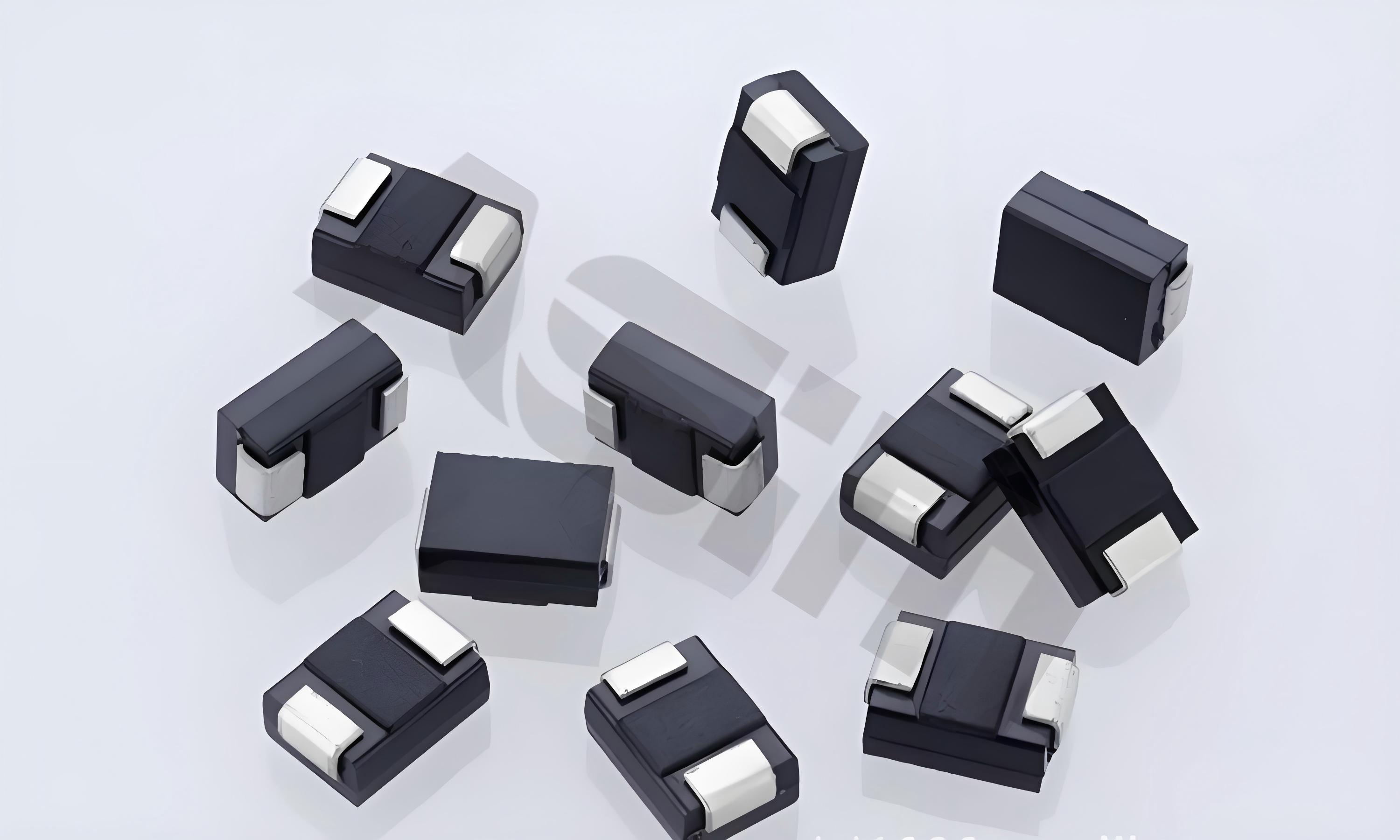
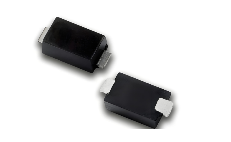
The four ASIM parts are useful for a constrained comparison because the working-voltage and clamp-voltage entries line up at their listed rating points. SMA04J24V is a 400 W SMA device with 10.3 A IPP. SMB06J24V is a 600 W SMB device with 15.5 A IPP, while SMB10J24V uses the SMB package and lists a 1000 W class with 25.7 A IPP. SMC15J24V is a 1500 W SMC device with 38.6 A IPP.
That does not create a simple “larger package wins” rule. The protected circuit sees the system transient plus the voltage caused by the board path between the TVS, its return, and the IC. A controller placed several centimetres from the TVS can still see a high local excursion while the TVS terminal reading looks acceptable. A long probe ground lead can also create a misleading waveform. Use a low-inductance probing method and record the same measurement point for every candidate.
For a nominal 24 V input, first establish the highest continuous voltage at the board connector. Include supply tolerance, charging mode, load-dump assumptions where applicable, and any overshoot that exists in the actual product. VRWM must cover that continuous condition. Then compare the downstream absolute maximum rating with the clamp behavior at the pulse condition being evaluated. A TVS does not make a circuit immune to a sustained wiring fault; upstream fusing, current limiting, and thermal behavior remain separate design checks.
The package choice also changes layout reality. SMA takes less area and can be considered where the expected pulse and thermal path fit its data-sheet limits. SMB provides two listed power classes in this comparison without moving to the SMC footprint. SMC needs more board area, but its higher listed pulse-current point can matter when the validated transient calls for it. Do not replace an SMA footprint with an SMC assumption during a late ECO: land pattern, copper area, assembly profile, and the return connection all change.
Do not convert the wattage label into an energy claim
Peak pulse power is tied to a defined transient waveform. Energy depends on the integral of voltage and current over time, not only on the peak product. Two pulses with the same peak can impose different thermal stress when their duration or shape differs. Repetition interval also matters because the junction may not return to its initial temperature between events.
A sustained overvoltage is a different fault. If an upstream source keeps the TVS in avalanche, the device can overheat even when the instantaneous current appears below a peak pulse rating. Fusing, current limiting, disconnect control, and fault duration belong in the input-stage review. The TVS cannot replace them.
When a surge generator is used, record the open-circuit voltage, short-circuit current, source impedance, waveform, coupling path, polarity, interval, and number of applications. When the disturbance comes from a real cable or motor load, measure the actual branch current rather than assigning the generator's nominal voltage directly to the TVS.
Use this short release record with the waveform files:
actual maximum continuous input voltage at the connector;
selected model and the exact data-sheet condition used for VC and IPP;
fuse or current-limit location relative to the TVS;
voltage measured at the TVS and at the protected IC input;
function, leakage, temperature, and repeat-stress result.
The release decision belongs to the tested board configuration. A 24 V TVS comparison narrows candidates; it cannot replace the surge plan for the whole input stage.
Validation evidence for the release record
Use a fixed test configuration before comparing candidates. The record should name the sample revision, cable type and length, supply setting, load state, firmware version, ambient condition, and measurement point. Record the original waveform before changing the device or layout. Change one variable, repeat the same test, restore the original configuration, and repeat it again. This A/B/A sequence is more useful than a single improved screenshot because it exposes changes caused by cable movement, probe placement, or operating state.
Keep electrical evidence and functional evidence together. Electrical evidence includes the voltage at the entry and the protected pin, current where appropriate, and the exact pulse or discharge condition. Functional evidence includes communication errors, reset events, leakage, standby current, temperature, and recovery after repeated stress. A passed bench pulse does not close the review if normal operation is degraded. Conversely, a clean function test without the relevant electrical condition does not prove clamp margin.
The approved part number therefore belongs with a specific footprint and layout revision. If either the footprint, return path, cable arrangement, or downstream circuit changes, reopen the comparison and verify the affected condition again.
The final record should connect the selected model, its conditions, its PCB location, and the verification result.
Original Author: ASIM Technical Team | Publisher: Shenzhen ASIM Electronics Co., Ltd.
Published: 2026-08-11|Updated: 2026-09-17
Copyright notice: Copyright belongs to Shenzhen ASIM Electronics Co., Ltd. Please retain the author, source, and original URL when quoting or republishing.
Original URL: https://asim.com.cn/tvs-24v-sma-smb-smc-comparison-en.html
 Previous