Submit






TVS diodes protect power inputs, exposed communication ports, inductive-load switching nodes, and long external cables from transient overvoltage. The application name defines the test scenario; it does not select the part by itself.
Direct answer
A valid selection starts with the highest continuous line voltage, the transient source, the specified waveform, the current that actually reaches the protection branch, and the maximum voltage tolerated by the downstream circuit. The same “24 V port” label can describe very different electrical stress.
Record the maximum continuous voltage and its duration.
Identify the required surge waveform, source impedance, and coupling path.
Compare maximum clamping voltage with the downstream absolute maximum rating.
Measure board-level residual voltage and inspect the part after stress.
Application map
| Location | Typical disturbance | Primary parameters | Board-level evidence |
|---|---|---|---|
| DC input | Switching or coupled surge | VRWM, VBR, VC, IPP, waveform | Residual voltage, current, temperature |
| External bus | Common- or differential-mode transient | Polarity, VC, capacitance | Receiver waveform and communication errors |
| Inductive load | Turn-off voltage | Repetitive pulse and thermal limits | Switch-node waveform and repetition rate |
| Long external cable | Coupled transient | Voltage window and return path | Cable configuration and recovery behavior |
Power inputs need a continuous-voltage window first
VRWM must remain above the voltage that the line has to sustain continuously. A TVS that conducts during a legitimate high-line condition can overheat before any surge occurs.
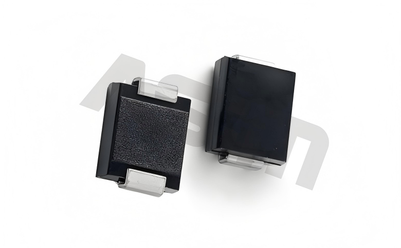
The ASIM SMA04J24V table lists 24 V VRWM, 26.7–29.5 V breakdown voltage at 1 mA, 38.9 V maximum clamping voltage, and 10.3 A peak pulse current under the datasheet condition. Those numbers describe one device condition, not every 24 V system.
Communication ports add signal and common-mode constraints
A device on an external bus must stay off across the normal signal and common-mode range. Capacitance, branch inductance, and the route to the reference plane can change the waveform seen at the transceiver.
Place the protection path near the entry point and measure at both the TVS and the protected IC. The voltage at the IC pin can exceed the datasheet clamp value because the PCB path adds inductive voltage.
Inductive loads require repetitive-pulse evidence
Relay coils, solenoids, and motors can generate repeated turn-off transients. A one-shot peak rating does not establish acceptable temperature under repetitive operation.
Capture the switching waveform, repetition interval, ambient temperature, and release-time requirement before choosing between a TVS, flyback diode, RC network, or an integrated clamp.
System surge tests and component pulse ratings answer different questions
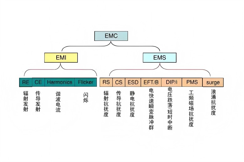
IEC 61000-4-5 defines a reproducible system-level immunity method. Component PPPM, IPP, and VC values belong to the waveform and conditions stated in the component datasheet. Keep both layers in the validation record instead of converting system kilovolts directly into a TVS wattage.
Save generator voltage, source impedance, and coupling mode.
Measure the current through the protection branch.
Monitor the protected rail and functional state.
Repeat leakage and functional checks after stress.
Questions engineers often ask
Can a power TVS protect a high-speed data lane?
Only if capacitance, topology, and insertion loss meet the interface requirement. A low-capacitance ESD protector is usually a different device class.
Does a higher peak-power number always provide more margin?
No. Peak power is waveform-specific and must be checked together with VRWM, VC, IPP, temperature derating, and the PCB return path.
Sources
Sources checked on October 10, 2026. Use the current datasheet revision and the approved test plan for final decisions.
 Previous