Submit






An ESD diode manufacturer's portfolio should be compared as a set of documented electrical windows, not as a model count. The useful evidence connects reverse working voltage, breakdown voltage, clamping voltage, pulse current, junction capacitance, package, and test conditions. A large catalog does not solve a design problem when its values cannot be traced to a specific part revision or measurement point.
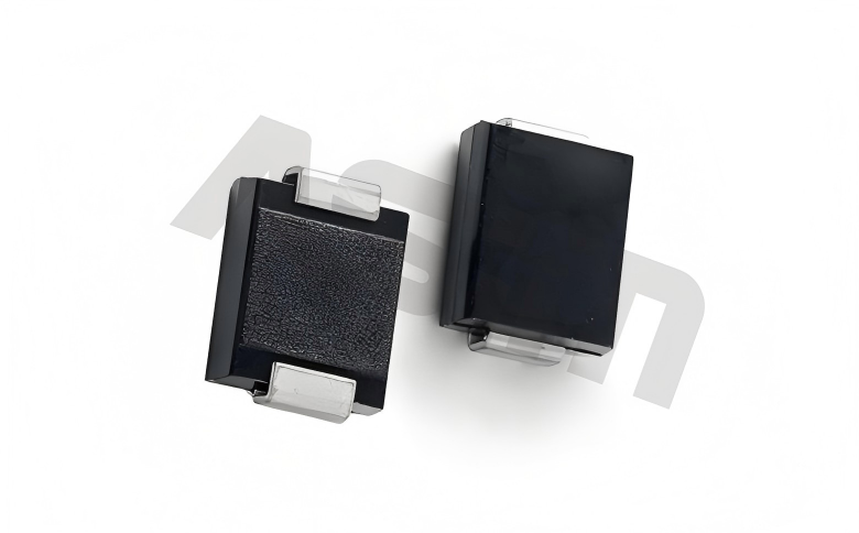
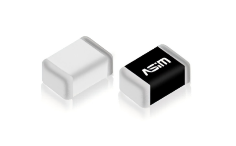
The four ASIM devices below illustrate why the selection cannot be reduced to “choose the lowest capacitance.” They share a bidirectional structure and a DFN0603-2L package, yet their operating-voltage and protection tradeoffs differ.
A portfolio table is a screening tool, not a release decision
| Part number | VRWM | Minimum VBR | Listed IPP | Maximum VC | Typical Cj | Polarity | Package |
|---|---|---|---|---|---|---|---|
| ESD1V1E003TA | 1.1 V | 1.4 V | 4.0 A | 8.0 V | 0.35 pF | Bidirectional | DFN0603-2L |
| ESD3V3E003TA | 3.3 V | 4.0 V | 4.0 A | 18.0 V | 0.30 pF | Bidirectional | DFN0603-2L |
| ESD5E001TA | 5.0 V | 6.0 V | 2.5 A | 18.0 V | 0.08 pF | Bidirectional | DFN0603-2L |
| ESD5E002TA | 5.0 V | 6.0 V | 3.0 A | 20.0 V | 0.18 pF | Bidirectional | DFN0603-2L |
These are catalog screening values from the current ASIM selection data. Maximum VC belongs to the listed IPP operating point, while Cj is a typical value. A design review still needs the current data sheet, the waveform and temperature behind the pulse values, the capacitance test condition, and the actual PCB result.
The table also shows why sorting one column is unsafe. ESD5E001TA lists 18.0 V maximum VC at 2.5 A. ESD5E002TA lists 20.0 V at 3.0 A. The current conditions are different, so the two voltage entries do not establish a universal clamping ranking. The same rule applies when comparing devices from different manufacturers.
Begin with the real operating voltage, including abnormal states that persist
VRWM is the reverse working voltage at which the device is intended to remain off, subject to its leakage specification. The system input must stay within that window during normal operation. “Normal” includes supply tolerance, power sequencing, common-mode bias, hot-plug behavior, and any fault voltage that can remain present long enough to heat the protection branch.
A 1.1 V device cannot be placed on a 3.3 V bus merely because its listed clamp voltage is lower. A 5 V device with very low capacitance is not automatically the best choice for a low-voltage IC either. The designer has to satisfy two separate limits: the diode must not conduct improperly during intended operation, and the protected pin must stay within its allowed transient stress during the specified event.
The protected IC's absolute maximum table is only part of that review. Check whether the limit applies to a powered or unpowered pin, how the input clamp network behaves, and whether the event is repetitive. The ESD diode's terminal voltage is not automatically the voltage at the IC. Package inductance and the PCB path between the diode, the return reference, and the protected node create additional overshoot.
Capacitance numbers need a measurement context
Typical junction capacitance is useful for shortlisting candidates. It does not describe the complete high-frequency branch. A meaningful comparison identifies the measurement frequency, DC bias, temperature, typical or maximum definition, port arrangement, and whether the value describes one channel or coupling between channels.
Consider the 0.08 pF entry for ESD5E001TA. It indicates a small nominal capacitive load under the stated device condition. It does not include the PCB pads, a routing stub, ground vias, connector discontinuity, or the remaining signal path. A long T-branch can consume more channel margin than the difference between two catalog capacitance values.
For a high-speed interface, request the following before using the part in simulation or a release review:
a Touchstone file tied to the complete part number and package revision;
port definitions, frequency range, fixture information, and de-embedding reference plane;
the bias, frequency, and temperature used for the capacitance data;
a recommended land pattern and return-path layout;
an explanation of whether the file includes the package and evaluation-board pads;
correlation data between the model or fixture and a physical sample.
An S-parameter file without its reference plane can produce a clean-looking simulation that is impossible to audit. The file may include part of a fixture, omit a land pattern, or represent a package revision different from the sample on the board.
Use the same evidence standard for an ASIM part and a competing part
A supplier comparison becomes biased when one device is judged from a detailed data sheet and another from a distributor table. Put every candidate into the same review form.
| Evidence area | Minimum information | What it supports | What remains a system task |
|---|---|---|---|
| Voltage window | VRWM, VBR range, breakdown test current | Off-state and breakdown screening | Actual operating range and IC stress limit |
| Clamp behavior | VC, corresponding IPP, waveform, temperature | Device-terminal behavior at a defined point | PCB overshoot and voltage at the protected pin |
| Signal loading | Cj conditions, S-parameters, port map | Device or fixture behavior at a stated reference plane | Eye, error rate, or link training on the target board |
| Production identity | Specification revision, lot identity, change notice | Whether documents match the delivered material | Incoming checks and requalification rules |
Application labels such as USB, HDMI, Ethernet, camera, or sensor interface are not substitutes for these fields. They may indicate where a device has been evaluated, but each target board still has its own voltage, routing, connector, and receiver margin.
Resolve document conflicts before sampling
Old selection guides, web product tables, and current data sheets sometimes disagree. The disagreement may come from a revised die, a package change, a changed pulse condition, a corrected table, or a simple transcription error. Do not select the most favorable value.
Freeze the complete orderable part number, document revision, publication date, and test point. Ask the manufacturer to identify which document applies to the sample lot. If the answer cannot be traced, remove that part from the comparison until the conflict is closed. A sample test is not a substitute for knowing what was sampled.
The same control is needed after qualification. A suffix change, wafer revision, assembly-site change, or data-sheet update can alter the evidence set even when the family name looks unchanged. Keep the approved specification, sample lot, PCB revision, and test record together.
A target-board comparison should isolate one variable
Catalog evidence narrows the candidates. The target board closes the decision. Prepare at least two equivalent boards or a rework plan that does not damage the pads. Hold firmware, cable, connector, power state, fixture, ambient condition, and measurement points constant.
A useful comparison sequence is:
Measure the unpopulated protection footprint or the approved baseline configuration.
Install candidate A and repeat the signal-integrity and protection tests.
Install candidate B without changing the surrounding layout.
Restore candidate A and repeat the measurement.
Compare the A/B/A spread with instrument repeatability and rework variation.
The restoration step matters. If the second A result does not reproduce the first, the apparent difference between A and B may have come from soldering, probe placement, connector wear, cable movement, or temperature. Do not publish an improvement percentage that is smaller than the measurement variation.
Electrical evidence and functional evidence belong in the same record. Electrical evidence includes the stress condition, current or voltage waveform, device-terminal voltage, and protected-pin voltage. Functional evidence includes link errors, resets, corrupted data, leakage, standby current, and behavior after repeated stress.
What a manufacturer statement can and cannot say
A defensible statement names the part, the conditions, and the boundary. For example: “The device lists a typical junction capacitance of 0.08 pF under its specified measurement condition and was evaluated on PCB revision X at the stated interface mode.” That statement can be audited.
“Supports all high-speed interfaces” cannot be audited. Neither can “the 18 V clamp protects any 5 V IC,” because the pulse current, waveform, PCB path, and IC limit are missing.
ASIM uses the same separation in its portfolio review: the selection table establishes candidates, the current data sheet defines component conditions, and the target-board record supports the application conclusion. A manufacturer earns engineering trust by keeping those three layers consistent, not by placing the largest number of interfaces beside a part number.
Original Author: ASIM Technical Team | Publisher: Shenzhen ASIM Electronics Co., Ltd.
Published: 2026-09-17
Copyright notice: Copyright belongs to Shenzhen ASIM Electronics Co., Ltd. Please retain the author, source, and original URL when quoting or republishing.
Original URL: https://asim.com.cn/compare-esd-diode-manufacturer-low-capacitance-portfolio-en.html
 Previous