Submit






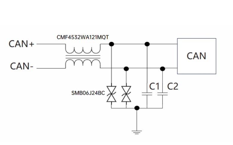
A 24 V industrial camera trigger input should not receive a TVS diode selected from the nominal voltage alone. The reverse working voltage has to cover the highest continuous terminal voltage, while the clamp voltage and PCB overshoot must remain inside the front end's transient limit. Trigger thresholds, pulse width, cable coupling, isolation, and the return path determine whether the result is a protected input or a camera that still takes false frames.
The failure is not always dramatic. The camera may remain powered and connected to the host while recording one extra frame, missing a trigger, extending an exposure, or incrementing an input counter. Looking only for reset or physical damage will miss these functional errors.
Reconstruct the input from the connector inward
Industrial cameras do not share one trigger circuit. A current model may accept a 12 V to 24 V signal through an opto-coupled input. Another camera may use an isolated digital receiver, a comparator, or a GPIO circuit referenced to an I/O ground. Some connectors carry trigger, strobe output, power, and ground in the same cable.
Before choosing the TVS, draw the path from the field connector to the logic domain. Identify:
the voltage reference for the trigger terminal;
the allowed continuous voltage range, including polarity and wiring faults;
high and low thresholds, input current, and hysteresis;
series resistance, current limiting, and existing input capacitance;
the reverse and pulse limits of the optocoupler LED, comparator, or receiver;
field-side, logic-side, chassis, and protective-earth relationships;
cable length, shield termination, and the shortest accepted trigger pulse.
This sketch usually reveals whether the protection device should return to an I/O reference or a chassis node. It also shows how much series impedance already exists. A large pulse-proof input resistor can limit TVS current, while a long trace between the connector and diode can add enough inductive voltage to raise the protected-node transient.
A “24 V” rail may exceed 24 V during normal service
Reverse working voltage, VRWM, is the continuous high-impedance boundary used for the initial TVS screen. If the field supply, tolerance, and permitted operating condition reach above 24 V, a 24 V VRWM part may sit too close to conduction. Leakage and temperature then become part of normal operation rather than an occasional transient issue.
The alternative is not simply to select the highest voltage available. Raising VRWM generally moves the breakdown and clamp window upward. A device that never conducts during normal operation can still allow too much voltage at the isolated receiver during a surge.
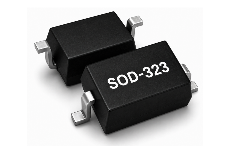
ASIM has SOD-123FL TVS entries with 24 V, 30 V, and 33 V reverse working voltages, including SODA24V-SH, SODA30V-SH, and SODA33V-SH. They illustrate the screening decision, not a universal camera recommendation:
| Candidate | VRWM | Question that must be answered before selection |
|---|---|---|
SODA24V-SH | 24 V | Does every allowed continuous input remain at or below this value? |
| SODA30V-SH | 30 V | Does the wider operating window still clamp below the receiver limit at the actual pulse current? |
| SODA33V-SH | 33 V | Is there enough transient margin after diode clamp and PCB overshoot are combined? |
Compare clamp voltage only at matched current, waveform, temperature, and data-sheet conditions. The protected node can see more than the diode's terminal voltage because the current path includes package, trace, via, and return inductance. Measure both locations when the margin is narrow.
False triggering is a threshold and time problem
An input circuit does not need to be damaged to make a bad decision. A disturbance only has to cross the receiver threshold for long enough to be accepted as a valid edge. The resulting frame can look normal, making the event difficult to connect with ESD or EFT exposure.
Use two synchronized observations when possible. Measure the protected terminal or the receiver input with one channel. Observe the isolated output, MCU capture pin, or event counter with another. If the terminal voltage is already limited but a logic pulse remains, replacing the TVS with a higher-power package may do little.
At that point, review the RC network, comparator hysteresis, optocoupler output pull-up, and firmware debounce or qualification time. Each change has a functional cost. Increasing capacitance may suppress a narrow disturbance while delaying a legitimate edge. A fast production line may reject a filter that looks perfectly adequate in a slow bench test.
The filter therefore needs a timing budget:
minimum valid trigger width at the connector;
cable and input-network delay;
rise and fall time at the receiver output;
firmware sampling or debounce interval;
maximum permitted exposure or acquisition delay.
Validate the shortest pulse and highest trigger rate after protection changes. A design that passes an immunity test but loses production triggers has not met the application requirement.
Isolation does not remove the system return path
Optical or galvanic isolation separates defined electrical domains. It does not make the connector immune to a discharge. Fast current can couple through the isolator's parasitic capacitance, the DC-DC converter, the enclosure, a cable shield, or a nearby ground structure.
The field reference, camera digital ground, metal enclosure, and protective earth may all be different nodes. Connecting the TVS to the wrong one can route current across the isolation barrier or lift a sensitive logic reference. Leaving the field side completely floating can allow a large common-mode voltage to develop elsewhere.
There is no universal ground symbol that solves this. Map the high-frequency current path for the actual mechanical assembly. A connector shell or shield should normally dispose of external current near the entry. A long pigtail from the cable shield to digital ground adds inductance and pulls the disturbance into the board.
If a controlled high-frequency connection is needed between domains, define its component, voltage rating, placement, and safety implications. Do not add an unreviewed capacitor across a certified isolation barrier.
Separate ESD, EFT, and wiring faults
The same connector can experience several stresses, but the protective response is not identical. A direct ESD event has a fast edge and may reach the connector shell or exposed pin. EFT can couple repeated bursts onto a long I/O cable. A wiring error can hold the terminal at an incorrect voltage for seconds or indefinitely.
A TVS diode handles a defined transient path. It does not replace reverse-polarity protection, current limiting, an eFuse, or a receiver designed for the allowed continuous input. Document each condition separately:
maximum permitted DC voltage and duration;
negative input or swapped-wire condition;
ESD test points and system setup;
EFT coupling method and cable configuration;
surge waveform and source impedance, when applicable.
Combining these conditions under one label such as “24 V transient” produces ambiguous requirements and usually an ambiguous test result.
Record camera behavior alongside PASS or FAIL
A repeatable test record should preserve the camera mode and the exact functional observation. Use a fixed lens or test scene if image continuity matters. Keep acquisition software, exposure, frame rate, trigger source, cable, and host connection unchanged between A and B tests.
Useful result fields include:
unexpected frames, missed triggers, or changed input counts;
link interruption and recovery time;
exposure or strobe state after the event;
reset-cause or error information available from firmware;
voltage at the diode and receiver-side measurement point;
leakage, breakdown, or other component checks after the sequence;
any temporary oscilloscope, debugger, or earth connection present during the test.
The last item is easy to overlook. An oscilloscope ground or communication cable can add a current-return path. A result obtained only with the measurement equipment attached must be reproduced in the normal product configuration.
Does every 24 V trigger input need a unidirectional TVS?
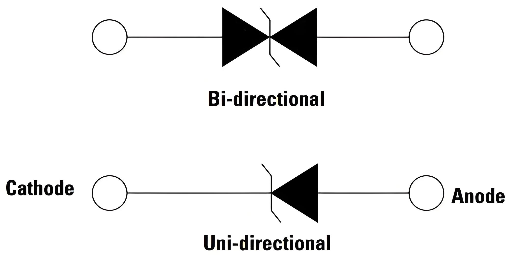
No. Polarity depends on the allowed signal, negative fault condition, and receiver circuit. A unidirectional TVS normally conducts forward for one polarity; a bidirectional part maintains a breakdown window in both directions. Select after defining the input waveform and fault range.
Is an opto-isolated input automatically protected from IEC ESD?
No. Isolation addresses a defined domain boundary. A system discharge can still use the connector, shield, enclosure, power network, and parasitic capacitance. The finished camera needs testing in its representative cable and grounding configuration.
Can a larger input capacitor replace the TVS diode?
The capacitor may reduce a narrow disturbance but also changes trigger timing and must withstand the event. It does not establish a controlled clamp voltage. Use it as part of a verified filter, not as an assumed substitute.
Original Author: ASIM Technical Team | Publisher: Shenzhen ASIM Electronics Co., Ltd.
Published: 2026-09-14
Copyright notice: Copyright belongs to Shenzhen ASIM Electronics Co., Ltd. Please retain the author, source, and original URL when quoting or republishing.
Original URL: https://asim.com.cn/industrial-camera-trigger-input-tvs-en.html
 Previous