





 Submit


How to implement CAN bus protection? A combination of ESD, TVS, and common-mode choke components.
 2026.07.25 00:00:00
 102
102





CAN bus protection is typically achieved through a combination of the transceiver's built-in protection, external ESD or TVS devices, optional common-mode chokes, and discharge paths near the connectors. ESD or TVS devices serve to limit transient voltages on the CANH and CANL lines, while common-mode chokes primarily suppress high-frequency common-mode noise; these components perform distinct functions and cannot replace one another.
Using more components does not necessarily result in greater stability; every protection component introduced into the CAN or CAN FD signal path adds junction capacitance, parasitic inductance, and impedance discontinuities. A sound design approach prioritizes meeting requirements for normal bus pin voltages and DC fault ranges, followed by an evaluation of transient clamping, signal integrity, and EMC. While the ASIM ESD24R003TA and CMF2012WE670MQT serve as examples for parameter verification, their suitability for a specific transceiver must be confirmed by applying the project's specific fault voltage levels and testing requirements.
First, distinguish between the three types of problems.
ESD events caused by connector mating/unmating or human contact are characterized by fast rising edges and short durations. An external TVS must provide a low-inductance discharge path before the current reaches the transceiver. External components are valuable when the system-level ESD requirement exceeds the transceiver's inherent capability, or when PCB layout conditions compromise the chip's built-in protection.
For transients generated by wire harness coupling, inductive load switching, and automotive electrical systems, the energy and duration may significantly exceed those of standard contact discharges. In such cases, the TVS current must be calculated based on the project-specified pulse waveform, source impedance, and repetition rate, rather than simply relying on the "ESD voltage rating" (e.g., "X kilovolts").
Common-mode interference manifests as simultaneous fluctuations in both CANH and CANL relative to the reference ground. A common-mode inductor presents impedance to this high-frequency current while allowing the differential-mode CAN signal to pass through with minimal obstruction. It serves to improve radiated emissions or immunity; it is not intended to absorb the full surge energy, nor is it a mandatory component for every CAN board.
The operating voltage of CAN protection devices must be determined based on their state relative to ground.
CAN communication relies on the differential voltage between CANH and CANL, yet protection devices may conduct from an individual bus line to ground. Therefore, when selecting the VRWM (Working Peak Reverse Voltage), one cannot simply consider the differential voltage swing; factors such as the common-mode range relative to ground for each bus line, node ground offset, and fault requirements regarding short-circuits to the battery or ground must also be taken into account.
For instance, if a transceiver is designed to withstand sustained DC fault voltages on the CANH or CANL lines, an external TVS that enters avalanche breakdown prematurely could inadvertently transform a sustained fault condition into a high-current path. This risks damaging the TVS, PCB traces, or upstream fuses rather than protecting the transceiver. From an engineering perspective, the following parameters should be compared on a single plot: the maximum bus-to-ground voltage likely to occur over an extended period; the TVS's working peak reverse voltage (VRWM) and leakage current range; and the absolute maximum and fault-tolerance ratings of the transceiver's bus pins.
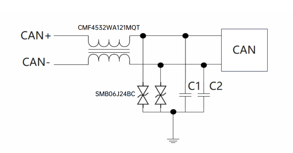
Bidirectional devices are commonly used on communication lines subject to AC swings or positive and negative transients; however, being "bidirectional" does not automatically make them suitable for CAN. It is still necessary to verify the clamping characteristics in both polarities, failure modes, and the symmetry between the two bus lines.
Low capacitance simply indicates that it is more signal-friendly.
The ESD24R003TA is a bidirectional SOT-23 device with the following specifications: VRWM of 24 V, minimum VBR of 25 V, IPP of 8 A (under specified conditions), maximum VC of 50 V, and a typical junction capacitance of 0.5 pF. The 0.5 pF capacitance is favorable for high-speed signal edges, making the device a suitable candidate for CAN and CAN FD applications.
However, this conclusion merely indicates that evaluation may proceed; it does not constitute direct approval for use. If the target transceiver cannot withstand a residual voltage in the vicinity of 50 V, or if the transient current exceeds the device's capabilities for the specific waveform and temperature, the component model or protection architecture must be adjusted. Conversely, if the system requires the bus to withstand a bus-to-ground fault exceeding 24 V for an extended period, it must first be verified that the device will not remain in a conducting state throughout the fault duration.
The clamping voltage (Vc) of a specific model—as specified in the datasheet for a given test current—does not necessarily equal the actual peak voltage experienced during an arbitrary pulse on the PCB. Parasitic trace inductance causes a voltage spike to be superimposed on the waveform during very fast rise times; consequently, the closer the measurement point is to the transceiver, the more accurately it reflects the actual residual voltage to which the chip is subjected.
The common-mode inductor should be determined based on EMC results.
The CMF2012WE670MQT features a 2012 package, a common-mode impedance of 67 Ω ±25% (at 100 MHz), a DC voltage rating of 50 V, a maximum DC resistance of 0.2 Ω, and a maximum rated current of 700 mA. This set of specifications is suitable for preliminary screening in CAN front-end applications; however, the 67 Ω figure represents the common-mode impedance at the specified frequency, not the series resistance for the CAN differential-mode signal.
Final component selection requires examining differential-mode insertion loss, S-parameters, leakage inductance, impedance-versus-frequency characteristics, transient current performance, and temperature profiles. CAN FD features faster edge rates; if differential-mode parasitic inductance is excessive, it may increase ringing, prolong zero-crossing times, or compress the eye diagram. Relying solely on the criterion that "higher impedance at 100 MHz is better" can easily lead to over-specification.
Common-mode inductors can store energy during bus short-circuits or transient events, potentially generating additional voltage spikes when the fault clears. Their placement relative to the TVS, the clamping path, and the transceiver's internal architecture must be verified as a system. If emission and immunity tests can be passed without the common-mode inductor, retaining a zero-ohm resistor or an optional mounting footprint often offers greater flexibility than mandating the component's installation.
What is the sequence for connecting the connector to the transceiver?
A common design approach is to route external energy entering via the connector through a protection node before it reaches sensitive areas on the board. The TVS return path should connect to the designated reference ground using a short, wide, and low-inductance trace; it must not loop across a large section of the PCB to reach a via. The CANH and CANL traces should be kept symmetrical, and the branches connecting to the protection devices should be matched in length as closely as possible.
Common-mode inductors are typically placed between the transceiver and the connector. The placement of the TVS diode relative to the inductor should not simply follow a reference design blindly: positioning it near the connector facilitates early shunting, whereas placing it near the transceiver can directly limit the voltage at the chip pins; the specific location affects the pulse stress on the inductor, the current loop, and the residual voltage. It is advisable to provide footprints for both locations on the prototype and determine the optimal placement based on measured waveforms.
Termination resistors, split termination capacitors, and TVS return paths collectively influence high-frequency currents. If the protective ground is connected to the system ground via a long, narrow copper trace, the transceiver's local reference potential may still rise due to ground bounce caused by the current, even when the TVS is conducting.
The selection of the combination can be advanced across four dimensions.
The first window concerns DC characteristics. Verify that CANH and CANL operate within the normal common-mode range and meet requirements regarding ground offset, short-to-battery, and short-to-ground conditions; rule out TVS components that might remain continuously conductive and common-mode chokes with insufficient current ratings.
The second window concerns transient characteristics. Estimate or measure the TVS shunt current based on specified waveforms, then compare the resulting maximum clamping voltage (VC)—accounting for temperature derating and PCB overshoot—against the transceiver's voltage withstand rating. Note that peak pulse current (IPP) values for different waveforms are not directly interchangeable.
The third window focuses on signal integrity. Check parameters such as bus capacitance, differential-mode insertion loss, return loss, signal edge characteristics, and eye diagrams. Passing tests for Classic CAN does not guarantee compliance for CAN FD, which involves higher data rates, longer wiring harnesses, or a greater number of nodes.
The fourth window involves vehicle-level or system-level testing. Conduct tests for ESD, conducted transients, radiated emissions, immunity, and DC faults, while recording transceiver functionality, bus error rates, TVS residual voltage, and component temperature rise. This approach allows you to determine whether issues stem from clamping capability, PCB layout, or filtering parameters.
Common errors often occur in the "individual component pass" requirement.
Simply removing all external protection because a transceiver is rated for high ESD tolerance may overlook the differences between chip-level test conditions and the actual application environment—such as connectors, wiring harnesses, and PCB layout. Similarly, a low TVS junction capacitance does not guarantee the device can withstand the high-energy pulses specified for the project.
Another mistake is selecting a high-impedance common-mode choke first and then attempting to fix signal integrity issues later. A more appropriate approach is to first determine the bus speed, topology, and specific EMC challenges, and then select a level of filtering that is sufficient without being excessive.
Component qualifications must also be verified independently. Meeting electrical parameter specifications does not automatically satisfy project requirements regarding automotive-grade certification, traceability, and temperature ratings. Before a component is included in the mass-production Bill of Materials (BOM), the latest official datasheet and certification documentation should be used as the definitive reference.
Common Questions About CAN Bus Protection
Do CAN transceivers with built-in ESD protection still require an external TVS?
Consider the system-level requirements, the degree of interface exposure, and the physical layout. If the transceiver's inherent capabilities—verified by actual system testing—meet the requirements, no additional protection is needed; however, if the connector interfaces directly with the outside world, the target protection level is higher, or the pulse energy is greater, an external TVS typically provides a more controllable discharge path.
Can a common-mode inductor replace a CAN TVS?
No. Common-mode inductors are used to suppress high-frequency common-mode currents, whereas TVS devices are used to limit transient voltages. Additionally, inductors may store energy during a fault event; therefore, the two components should be selected individually and tested in combination.
Is a 0.5 pF ESD device necessarily suitable for CAN FD?
Not necessarily. While low capacitance benefits signal integrity, one must also verify VRWM, VC, IPP, package parasitics, and transceiver voltage tolerance. Ultimately, CAN FD compliance depends on the eye diagram and bit error rate (BER) under the specific target data rate, wiring harness, and node conditions.
Is it better to place the TVS diode as close as possible to the transceiver?
Not necessarily. The protection circuit needs to be placed close to the energy entry point while ensuring that the residual voltage at the transceiver pins remains sufficiently low. Connectors, common-mode chokes, and grounding structures can alter the optimal placement; therefore, it is recommended to provide for design flexibility and verify the setup using an oscilloscope near the transceiver pins.
The actionable conclusion for CAN bus protection is to first define the DC fault window, then calculate the transient clamping window, and subsequently verify signal integrity and EMC. While the ESD24R003TA and CMF2012WE670MQT can be used to form a candidate combination, the specific models are truly suitable for the board only if all four windows are satisfied.
 Previous

Related News

2024.10.12
EMC testing Contents and Current Situation of Automotive Electronic products

2025.02.21
How to choose the best circuit protection devices in a circuit?
2026.07.08
What is the difference between SMA and SMB packaged TVS diodes?
2026.07.10
What is the difference between SMD TVS and leaded (through-hole) TVS?
2026.07.15
For what applications are SOD-323 packaged ESD diodes suitable?
2026.07.17
How should TVS diodes and common-mode inductors be configured for a CAN interface?
2026.07.17
How do you choose between SMA, SMB, and SMC packaged TVS diodes?
2026.07.20
For which automotive applications is the SM8S series TVS suitable?

2026.07.22
What issues need to be checked during EMC rectification?
2026.07.23
How do you implement ESD protection for USB Type-C interfaces? You need to select separate solutions for the data lines, CC lines, and VBUS.


