





 Submit


How do you implement ESD protection for USB Type-C interfaces? You need to select separate solutions for the data lines, CC lines, and VBUS.
 2026.07.23 00:00:00
 140
140





USB Type-C ESD protection must be implemented based on signal groups. SuperSpeed TX/RX, USB2 D+/D-, CC1/CC2, SBU1/SBU2, and VBUS serve different functions and operate with distinct normal voltages, signal rates, and fault conditions; therefore, it is inappropriate to apply a single set of parameters to all of them simply because they are "Type-C specific."
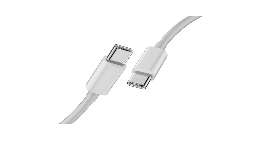
For high-speed data lines, prioritize junction capacitance (Cj), channel consistency, and package parasitics. For CC and SBU lines, account for potential accidental contact with VBUS; treat VBUS itself as a power input, focusing on verifying normal operating voltage, clamping, and the voltage tolerance of downstream components. Separate these signal groups in the schematic from the outset to avoid applying a single set of parameters across all lines.
First, verify exactly what functions are enabled on this Type-C port.
Type-C refers to the connector and its configuration system; it does not imply that every product supports the same data and power delivery capabilities. Some ports offer only USB 2.0 and basic power delivery, while others support SuperSpeed, USB Power Delivery negotiation, or Alternate Modes. Protection schemes should be based on the specific port capabilities rather than simply populating components for all 24 pins.
SuperSpeed TX/RX lines are used for high-speed differential transmission. While the USB 2.0 D+/D- lines operate at lower speeds than SuperSpeed, they still serve as data lines. CC1/CC2 handle connection detection, orientation recognition, and communications related to roles and power delivery; SBU1/SBU2 carry auxiliary signals for certain Alternate Modes or accessory functions. VBUS connects directly to the power path.
SuperSpeed or SBU pins that are not enabled based on the port configuration should not be forcibly connected to the array simply to meet a specific lane count. CC1 and CC2 pins cannot simply be treated as "No Connect" (NC): once a connection is established, one pin is used for CC communication, while the other may be required to supply VCONN power. For any lines connected to controllers, multiplexers, or external contacts, both normal and fault conditions must be verified individually.
For SuperSpeed TX/RX, both low capacitance and differential symmetry must be considered.
When an ESD device is connected between a high-speed line and ground, its junction capacitance becomes part of the signal path. Excessive capacitance, a mismatch in capacitance between the two lines, or significant asymmetry in package pads can all increase signal loss and the risk of reflections. While "ultra-low capacitance" serves as a useful initial screening criterion, it cannot replace a comprehensive evaluation of interface data rates, trace lengths, and the complete signal channel.
For multi-channel arrays, pinout configuration is also a critical factor. A package suited for flow-through routing allows differential lines to enter from the connector, pass through protection pads, and proceed directly to the interface chip. If the device forces the lines to take a detour, change layers, or extend into long stubs, the resulting parasitic effects cannot be compensated for simply by having a low nominal junction capacitance (Cj).
Although Type-C connectors support reversible insertion—which involves switching active data lanes—routing requirements remain stringent. For each TX/RX pair, differential routing must be maintained, the reference plane must be continuous, and the length of unprotected traces preceding protection components should be minimized.
For USB 2.0 D+/D-, there is no need to replicate the implementation used for SuperSpeed devices.
For USB 2.0 D+/D- lines, junction capacitance must also be controlled, though the selection margins and PCB requirements differ from those of SuperSpeed. In addition to junction capacitance (Cj), factors such as reverse working voltage, clamping performance, leakage current, package type, and grounding structure must be verified. High-capacitance TVS diodes intended for power ports should not be placed directly on the D+/D- lines.
While there are indeed arrays capable of covering USB 2.0, SuperSpeed, and control lines simultaneously, the voltage window, junction capacitance (Cj), and internal structure of each channel must be verified individually. If even one set of parameters fails to meet requirements, it is better to select separate components rather than forcing other lines to compromise just to save on a single device.
CC and SBU must not be protected against electrostatic pulses alone.
The CC and SBU pins are located in close proximity to the VBUS pin. Connector damage, foreign objects, moisture, or skewed insertion/removal can all lead to accidental contact. While standard ESD diodes are effective at handling brief electrostatic pulses, they are not designed for continuous overvoltage protection; subjecting them to prolonged power-supply energy absorption can cause the device itself to enter a hazardous state.
The operating window for CC1/CC2 must encompass connection detection, power delivery/communication, and VCONN-related states. For any exposed Type-C port, the risk of misconnection must be assessed based on the actual maximum VBUS voltage; when supporting higher negotiated voltages or Extended Power Range (EPR), the connector's voltage withstand rating, cutoff capability, and transient overshoot characteristics must be verified—legacy designs intended only for low-voltage ports cannot be reused.
If the CC path is routed through a port protection switch, the side supplying VCONN must also be evaluated for current-carrying capacity, on-resistance, and voltage drop. Relying solely on ESD ratings is insufficient to determine whether connection and power delivery functions are operating correctly.
SBU requirements should be assessed based on actual functionality. When Alternate Modes are enabled, bandwidth and junction capacitance become key selection criteria; even when such functions are not enabled, the handling of these pins on both the connector and system sides must still be verified. The fact that CC and SBU pins are adjacent does not imply they necessarily utilize the same voltage rating or the same component.
The VBUS design is based on the power input.
Protection devices on the VBUS must accommodate the highest normal operating voltage the port might encounter, while allowing sufficient margin for normal fluctuations. For ports supporting power delivery negotiation, TVS selection cannot be based solely on the default power state; otherwise, significant leakage or premature conduction may occur when the bus voltage rises.
There is no need to aim for the ultra-low capacitance levels required for data lines here. More relevant parameters include reverse working voltage, clamping voltage under specified conditions, pulse-handling capability, package thermal dissipation, and the voltage tolerance of downstream power chips. Issues such as port directionality, overcurrent, reverse current injection, and sustained overvoltage should be handled by appropriate power switches or protection circuits.
Although the VBUS copper trace is typically wide to handle high currents, the TVS loop path must still be kept short. Moving the component deep onto the board to accommodate a larger package creates a longer path between the power input and the protection point.
How to route USB Type-C ESD protection on a PCB?
High-speed lines from the Type-C connector should first enter the protection array before connecting to the multiplexer or main controller. Do not connect the TVS as a branch off the main signal line after it has already entered the PCB. Ground the array's ground pin nearby, and keep the trace segment preceding the protection component as short as possible.
The connection method for the shielding shell, chassis ground, and digital ground must comply with the system-level grounding scheme. Simply connecting all TVS devices to the same "GND" net does not guarantee that electrostatic discharge (ESD) currents will follow the intended path to ground.
When selecting Type-C protection devices, ASIM first identifies which channels are enabled on the port, then considers parameters such as maximum VBUS voltage, downstream voltage tolerance, Alternate Mode requirements, and available package space. Specifying only "USB-C interface" is insufficient, as it fails to define critical details like the number of channels or CC pin overvoltage protection requirements.
Frequently Asked Questions
Can a single ESD array protect all Type-C signal pins?
While suitable shared arrays exist, the number of channels is just one factor; operating voltage, junction capacitance (Cj), internal clamping architecture, and pinout configuration must all align, and the VBUS line should still be handled separately.
If ESD diodes are already used on the CC lines, is overvoltage protection still required?
While appropriate ESD devices can handle electrostatic pulses, a sustained short-circuit to VBUS represents a different type of fault. Exposed ports should be evaluated for isolation and overvoltage protection capabilities based on the actual maximum VBUS voltage, with dedicated port protection solutions employed if necessary.
Should the TVS on the VBUS line also be a low-capacitance type?
Low capacitance is not the primary concern. Since VBUS is a power line, factors such as normal operating voltage, clamping conditions, pulse handling capability, and the voltage tolerance of downstream components are more important.
What is the ideal distance (in millimeters) between the Type-C protection device and the connector?
There is no need to aim for a specific, fixed distance. The priority is to ensure the signal path reaches the protection node immediately after leaving the connector—keeping the trace segment before the protection device as short as possible—while avoiding any disruption to the differential pair just to get closer to the connector.
 Previous

Related News

2024.10.12
EMC testing Contents and Current Situation of Automotive Electronic products

2025.02.21
How to choose the best circuit protection devices in a circuit?
2026.07.13
How do I select a 5V low-capacitance ESD diode model?
2026.07.15
For what applications are SOD-323 packaged ESD diodes suitable?
2026.07.17
How do you choose between SMA, SMB, and SMC packaged TVS diodes?
2026.07.20
How should a failure in the CAN communication surge test be handled?
2026.07.20
For which automotive applications is the SM8S series TVS suitable?
2026.07.20
How do you design a TVS protection solution for automotive power supplies?

2026.07.22
What issues need to be checked during EMC rectification?
2026.07.22
What is the difference between ESD arrays and single-channel ESD devices? A selection guide for multi-channel interfaces.


