High-frequency Circuit TVS Diode Junction Capacitance Optimization Strategy -ASIM
Optimization strategy for junction capacitance of TVS diodes in high-frequency circuits and ESD protection balance scheme
Core contradiction: The triple impact of junction capacitance on high-speed systems
1.1 Quantitative model of signal attenuation
The physical relationship between insertion loss and junction capacitance:

Among them:
- f:Signal frequency (GHz)
- Cj:Junction capacitance (pF)
- Z0:Transmission line impedance (Ω)
Measured influence:
In a 56Gbps PAM4 system:
- When Cj>0.3pF, the height attenuation of the eye diagram is greater than 40%
- For every 0.1pF increase in capacitance, the signal-to-noise ratio deteriorates by 3dB
1.2 Time-domain distortion mechanism
- Signal rise time degradation formula: ▲Tr = 2.2CjZ0
- In the 28GHz frequency band:
- Cj=0.5pF ⇒ Group delay fluctuation>5ps
- Cj=0.1pF ⇒ Group delay fluctuation<1ps
Five core technical paths
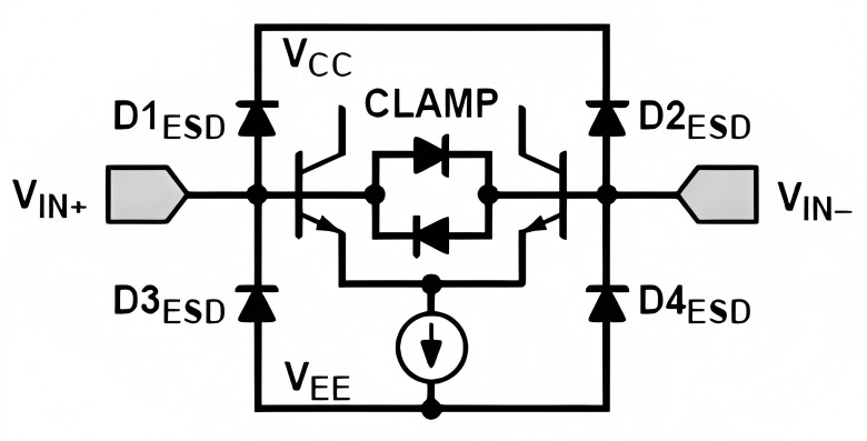
2.1 Wafer-level structural innovation
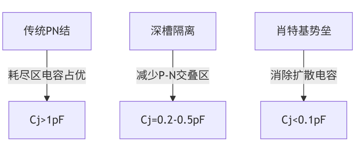
Process comparison:
- Deep groove isolation: Groove depth 30μm/ width 1μm, breakdown voltage increased by 200%
- Schottky structure: The thickness of the gold-half contact interface is less than 10nm, and the response time is 0.1ns
2.2 Advanced packaging technology
Performance evolution
| Encapsulation type | Parasitic inductance | Maximum applicable frequency | S21 loss @40GHz |
|---|---|---|---|
| Wire bonding | 1.5-2nH | <10GHz | -4.2dB |
| Upside-down welding | 0.5-0.8nH | 40GHz | -1.8dB |
| Copper column interconnection | 0.15-0.3nH | >100GHz | -0.5dB |
Scenario-based design specifications
3.1 Frequency band adaptation matrix
| Application scenarios | Maximum Cj | Structural requirements | ESDindex |
|---|---|---|---|
| Sub-6GHz | ≤0.5pF | Guard ring Isolation | ±25kV |
| mmWave | ≤0.1pF | Distributed diode array | ±30kV |
| 112G Optical module | ≤0.05pF | MEMS Integrated process | ±15kV |
3.2PCB Collaborative design
The Golden Rule:
- Layout:
- TVS distance protection point ≤λ/20 (λ: minimum wavelength)
- The spacing of grounding holes should be less than 0.25 times the thickness of the plate
- Impedance control:
- Use a coplanar waveguide (CPW) structure
- Impedance tolerance control ±3%
- Thermal management:
- Each watt of surge power requires 8mm² copper foil
- Avoid the solder mask covering the heat dissipation path
Verification methodology
Core standard
| Test project | Industrial standard | Attainment threshold |
|---|---|---|
| TDECQ | IEEE 802.3ck | ≤3.0dB |
| EVM | 3GPP 38.104 | ≤8%@28GHz |
| High eyes | OIF-CEI | ≥70mV@112G |
Engineering decision tree
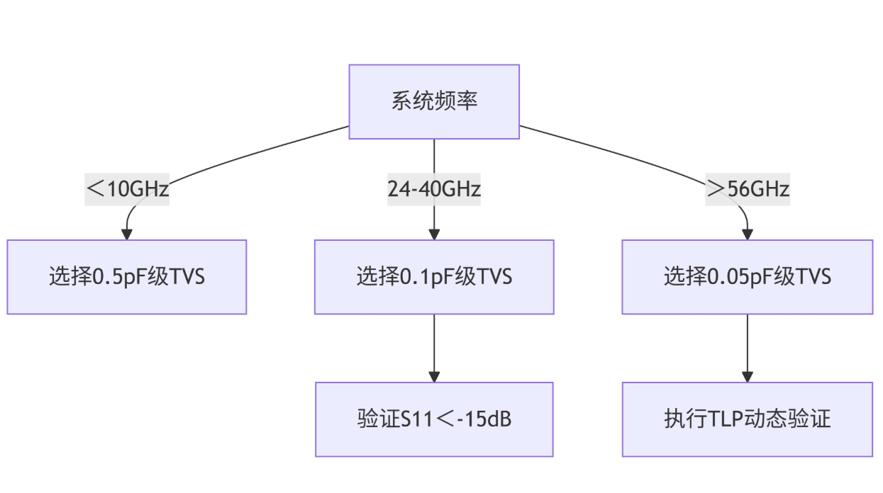
Innovative conclusion
Three major breakthroughs need to be achieved for the optimization of high-frequency TVS junction capacitors:
- Material breakthrough: Asymmetric doping was adopted to reduce the depletion region capacitance by 40%
- Structural revolution: Distributed microdiode arrays to disperse capacitive loads
Verification: The optimized scheme achieves insertion loss < 0.8dB, ESD protection ±30kV (IEC 61000-4-2 Level 4) in the 28GHz frequency band, and the bit error rate meets the requirements of the 3GPP URLLC standard.


