Submit






An ESD diode cannot be selected from an interface name and a system test level alone. A usable request identifies the line's full operating-voltage window, signal polarity and mode, protected-pin limit, channel configuration, PCB entry path, and system-level ESD target. “Type-C, 8 kV, low capacitance” leaves each of those decisions open. The checklist below turns that short request into conditions that can be reviewed and tested.
Start with the missing inputs, not a preferred part number
The quickest way to create a weak selection is to begin by searching a catalog for the lowest capacitance or the highest ESD rating. Begin instead with the circuit and the verification target. This table can be copied into a design review, sample request, or failure-analysis intake form.
| Input field | What to record | Why it changes the selection |
|---|---|---|
| Operating-voltage window | Minimum, nominal, and maximum continuous voltage; power-up, power-down, hot-plug, and sustained abnormal states | Establishes the VRWM margin and the risk of leakage or unintended conduction |
| Polarity and common-mode range | Unipolar or bipolar signal, DC bias, and upper and lower common-mode limits | Determines whether a unidirectional, bidirectional, or array topology is appropriate |
| Protocol and active mode | Protocol revision, actual data rate, lane configuration, and modes used in the product | The interface name alone does not define spectrum, timing margin, or receiver behavior |
| Channels and pins | Number of lines, differential pairs, shared nodes, direction, and connector pin map | Prevents channel-count, pinout, and routing errors |
| Protected-device boundary | Absolute maximum for the relevant pin, power-state conditions, and known internal protection behavior | Creates a boundary for residual-voltage verification |
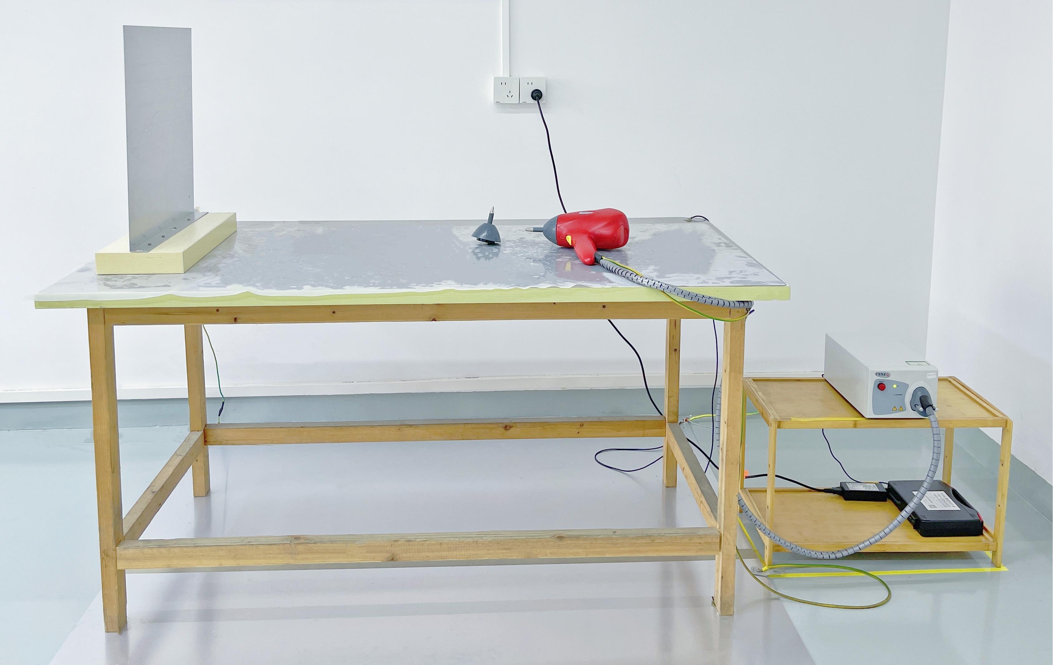
| System ESD target | Applicable standard revision, contact or air discharge, level, points, polarities, repetitions, and performance criterion | Separates a component specification from a reproducible equipment test |
| PCB implementation | Connector position, protection location, entry trace, return path, stack-up, and ground vias | Determines whether transient current reaches the protection branch before the sensitive circuit |
| Project state | Schematic design, first prototype, failed test, production replacement, or cost review | Determines whether paper screening, board comparison, or failure reproduction is required |
An incomplete form can still produce a provisional shortlist. It should not produce a released bill of materials. In particular, an unknown protected-pin limit or an unreviewed return path prevents a defensible clamping conclusion, even when the diode data sheet appears complete.
Why a system-level “8 kV” target does not select an “8 kV diode”
A system ESD immunity test describes a generator, discharge method, application point, test sequence, and product performance criterion. A diode document may describe component-level withstand, peak current under a defined transmission-line pulse, or clamping voltage at a specified current. Those results answer different questions.
Keep three layers separate:
What stress is applied to the finished equipment, and where can it enter?
What current and voltage develop in the external protection branch?
What residual stress reaches the protected semiconductor pin?
There is no responsible one-step conversion from a system discharge voltage to a diode part number. Trace inductance between the connector and protection device, inductance in the return path, any series impedance, package parasitics, and the IC's internal network all affect the waveform at the sensitive node. A diode that survives a component test may still be ineffective in a poor layout. Conversely, a lower component label does not by itself establish that a well-designed system will fail.
Write the system level in the checklist because it defines the validation objective. Do not copy it into the component-rating column as though the two tests were interchangeable.
Read six electrical parameters with their conditions attached
The following abbreviations are useful screening fields. None should be copied without its test context.
| Parameter | Screening question | Conditions that must stay attached | What it cannot prove by itself |
|---|---|---|---|
| VRWM | Within what voltage window is the device intended to remain off? | Polarity, continuous maximum, temperature, and leakage definition | Safe voltage at the protected IC pin |
| VBR | At what voltage does breakdown occur at a defined current? | Breakdown test current, minimum/typical/maximum definition, and temperature | Dynamic clamp voltage during the target transient |
| VC | What voltage is listed at a specified pulse current? | Corresponding IPP, waveform, pulse width, temperature, and limit type | Voltage at the IC after PCB overshoot |
| IPP | What peak pulse current is listed for the device? | Waveform, duration, repetition, and temperature | Superiority over a value measured with a different waveform |
| Cj | What nominal capacitive load does one device or channel present? | Frequency, DC bias, temperature, port arrangement, and typical or maximum definition | Complete channel insertion loss or eye margin |
| IR | What leakage is specified at a stated reverse voltage? | Applied voltage, temperature, and maximum-value definition | Leakage or power in every system state |
Suppose two candidate sheets both list 18 V clamp voltage. If one value is measured at 1 A and the other at 5 A, the entries do not establish equal behavior or a fair ranking. The same discipline applies to capacitance. Two “0.2 pF” values are not necessarily comparable when the bias, frequency, port configuration, or statistical definition differs.
A robust internal spreadsheet places the value and its condition in adjacent columns. It also records the document revision and complete orderable part number. This prevents a distributor table, an old selection guide, and a current specification from being blended into a number that belongs to none of them.
There is no universal Cj threshold for every high-speed interface
Low junction capacitance is often necessary on high-speed signal lines, but “Cj below X pF” is not a complete acceptance rule. The outcome depends on the signal spectrum, bias dependence, package pads, branch length, differential discontinuity, return-reference geometry, connector, and receiver margin. Two products using the same protocol can operate at different modes and have very different channel budgets.
Before treating a capacitance value as comparable evidence, ask for:
whether the number is typical or maximum;
measurement frequency, DC bias, temperature, and channel definition;
a Touchstone file tied to the complete part number and package;
port mapping, frequency range, fixture description, and de-embedding plane;
clarification of whether evaluation-board pads or a fixture remain in the model;
the recommended land pattern and return-path arrangement.
The PCB can outweigh a small difference between catalog values. A very low-capacitance diode connected through a long T-branch still creates a discontinuity. Large pads, a necked trace, an interrupted reference plane, or a long ground route can consume channel margin that the nominal Cj number never described.
For this reason, use Cj to screen, S-parameters to inspect frequency-domain behavior, and a target-board test to close the signal-integrity decision. Without the real board and active mode, avoid an unconditional statement that a particular capacitance “supports” a particular data rate.
Package review is an electrical review
Package selection is not the last mechanical checkbox. It determines whether the device can sit close to the entry point, whether the signal can pass through without a long stub, and whether the transient return can reach a continuous reference with low inductance.
Check all of the following before approving a footprint:
signal pin order and whether the differential pair can remain geometrically balanced;
ground-pin position, trace width, via count, and distance to the reference plane;
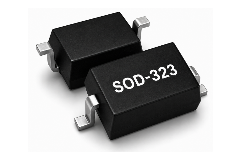
land-pattern dimensions, solder-mask opening, assembly capability, and rework access;
array channel order and any shared-pin topology;
package height and keep-out requirements near the connector;
whether a production replacement can use the same footprint without changing the electrical path.
If the diode is placed far from the connector, the discharge current can travel past the intended branch before it is diverted. If its return trace loops around a split or passes through a single distant via, the data-sheet clamp voltage does not automatically appear at the protected node. Review the placement while selecting the device, not after an immunity failure.
Four verification layers, four different decisions
A strong selection workflow does not ask one test to answer every question.
| Layer | Primary inputs | Decision it supports | What it does not replace |
|---|---|---|---|
| Data-sheet screening | Voltage window, VBR, VC/IPP, Cj, IR, package, temperature conditions | Removes clearly incompatible devices and forms a shortlist | Target-board signal testing or equipment ESD testing |
| S-parameter review | Part-specific file, port map, reference plane, channel model | Compares modeled frequency-domain loading under stated assumptions | Physical pads, connectors, manufacturing variation, and bench correlation |
| Target-board signal test | Same PCB revision, operating mode, cable, fixture, and instrument setup | Shows whether the assembled candidates change the actual link | System-level immunity performance |
| Equipment ESD test | Controlled sample, firmware, mode, discharge point, polarity, repetitions, and criterion | Shows product behavior under the defined system test | Proof that one diode is the only cause of a pass or failure |
For a close comparison, keep an approved baseline and use an A/B/A sequence. Measure candidate A, install candidate B without changing the surrounding path, then restore candidate A and repeat the measurement. If the restored A result does not reproduce the first A result, the apparent A-to-B difference may come from rework, connector wear, cable movement, probe placement, or temperature.
Record electrical and functional observations together. Electrical observations may include the stress waveform, diode-terminal voltage, protected-node voltage, and return-current path. Functional observations may include link errors, resets, display disturbance, corrupted data, abnormal standby current, or recovery behavior. Neither category is sufficient when the other is missing.
A selection example should expose assumptions, not imitate customer data
Consider a hypothetical high-speed differential input whose exact receiver limit is not yet available. The product team provides a protocol name, a nominal rail, and an 8 kV system target. This is not enough to recommend a released part.
The responsible output at this stage is a gap list:
capture the maximum signal swing and common-mode range in powered and unpowered states;
obtain the protected-pin transient boundary or agree on a board-level measurement limit;
identify the active data rate and channel compliance metric;
freeze the connector-to-diode and diode-to-reference layout;
define the discharge points, modes, repetitions, polarities, and performance criterion;
compare part-specific models and then verify the shortlist on the board.
Calling that result “candidate range pending verification” is accurate. Calling it “a proven 8 kV solution” would invent evidence that the project has not produced. This article therefore does not publish a product comparison table made from unverified catalog values.
Information required for a reviewable shortlist
The submission does not have to be a polished report. It does need to identify one board revision and one operating configuration. Provide:
interface name, protocol revision, active mode, target rate, and channel count;
minimum and maximum continuous voltage, common-mode range, polarity, and hot-plug behavior;
the protected IC's complete part number, relevant pins, and available stress limits;
local schematic plus PCB images showing the connector, protection footprint, sensitive node, reference plane, and return vias;
applicable system ESD standard revision, discharge method, target level, points, polarities, repetitions, and performance criterion;
for an existing failure, the reproducible symptom, sample and firmware revision, discharge condition, and recovery method;
package height, land-pattern space, sourcing constraints, and production-replacement requirements.
Missing inputs should remain visible in the decision record. Do not silently replace them with a familiar value from another project. The output can then separate three groups: incompatible devices, candidates worth simulating or sampling, and conditions that still require measurement.
Submit the interface conditions and review the candidate range
Combine the operating window, signal mode, protected-pin boundary, PCB entry and return path, and equipment test target in one request. The ASIM Technical Team can then move the review from “find a low-capacitance diode” to “identify which candidates justify board testing and what remains unproven.” Release the selection only after the current formal specification, target-board signal result, and equipment ESD result agree.
Original Author: ASIM Technical Team | Publisher: Shenzhen ASIM Electronics Co., Ltd.
Published: 2026-09-18
Copyright notice: Copyright belongs to Shenzhen ASIM Electronics Co., Ltd. Please retain the author, source, and original URL when quoting or republishing.
Original URL: https://asim.com.cn/esd-diode-selection-checklist-en.html
 Previous