





 Submit


Why does the ESD test still fail after replacing the protection device? Troubleshooting discharge paths, grounding, and component placement.
 2026.07.29 00:00:00
 94
94





If an ESD fix fails even after replacing the protection component, the issue is rarely just a matter of the component lacking sufficient capacity. The ESD current might be bypassing the component to enter the motherboard, or the branch path from the component to the return point could be too long. Alternatively, the component might be triggering correctly, yet the actual clamping voltage still exceeds the tolerance of the downstream circuitry.
Troubleshooting requires examining three specific points: the connector entry, the terminals of the protection component, and the pins of the protected chip. Simply comparing the nominal ESD ratings of two components does not reveal the actual path the current takes on the board.
First, determine whether the protection device is connected to the actual entry point.
An interface connector is generally not an ideal node. Its metal shielding shell, signal pins, power pins, and mounting tabs may connect to different reference points. If an ESD gun discharges onto the shielding shell, the current does not necessarily flow through the signal line's TVS; conversely, a discharge onto exposed pins could allow the current to travel directly along the signal trace into the transceiver.
Map out the current path based on the actual discharge point rather than relying solely on the schematic. While the schematic might show the TVS placed right next to the interface, the actual PCB layout could interpose traces, vias, or common-mode components between them. If a protected trace passes through the mainboard area before branching off to the TVS, the ESD wavefront will reach both the TVS and the downstream chip simultaneously.

When performing verification using temporary shorting, trace cutting, or localized shielding, alter only one primary path at a time. If a specific modification proves effective, it indicates that the approach is worth pursuing; however, this does not mean the temporary connection method is suitable for direct mass production.
Why "being close to the interface" may still not be enough
Although a protection device may be physically close to the connector, its discharge path can be quite long. The ESD current path encompasses signal traces, the device package, ground pads, vias, planes, and chassis connections; parasitic inductance in any of these segments introduces an additional voltage drop.
For rapidly changing currents, the voltage depends on path inductance and the rate of change. A long, thin ground trace may exhibit negligible voltage drop under DC conditions yet generate a high transient potential during the ESD leading edge. Consequently, even though the protection device has triggered, downstream pins may still experience significant voltage overshoot.
During layout reviews, do not simply measure the straight-line distance from the connector to the TVS; instead, measure the full path length from the TVS to the high-frequency return point. Prioritize minimizing branch lengths, the number of vias, and the return loop area.
Digital ground is not the ideal destination for all ESD currents.
Many circuit boards connect protection devices directly to a large digital ground plane, operating under the assumption that more copper equates to greater safety. The issue arises because this same digital ground plane also serves the MCU, power supply, crystal oscillator, and interface transceivers. When a high current is injected, the local potential across the ground plane shifts rapidly, causing the reference voltage seen by sensitive circuits to fluctuate accordingly.
When a metal chassis or connector shielding is present, high-frequency currents at the entry point should ideally complete their circuit path through the chassis or shield; the relationship between chassis ground and circuit ground should then be managed via a deliberate connection design. In the absence of a metal chassis, one must still clearly define the return path—whether via power lines, communication lines, or parasitic capacitance—to the test reference plane.
"Keeping chassis ground and digital ground completely isolated" is not a universal solution either. Decisions regarding connection points, contact areas, and the use of capacitors or impedance elements must be made by balancing safety requirements against considerations for low-frequency ground loops and high-frequency return paths. The worst-case scenario during ESD remediation is a schematic that depicts two separate grounds, yet lacks a definable return path within the PCB layout or mechanical structure.
Matching device parameters does not mean the clamping is safe.
When selecting protection devices, the VRWM must accommodate the interface's maximum normal operating voltage and any permissible DC offset; the clamping voltage (VC) under actual transient current conditions must remain below the downstream circuitry's tolerance threshold. The breakdown voltage (VBR) merely marks the onset of the avalanche region and should not be treated as the final clamping voltage.
The VC and IPP values specified in device datasheets must be interpreted in the context of the defined pulse conditions; ESD pulses, 8/20 μs current pulses, and other surge waveforms are not directly interchangeable. Furthermore, due to parasitic effects from PCB traces and component packaging, the peak voltage at the chip pins may exceed the test values listed in the datasheet.
For high-impedance or high-speed interfaces, factors such as junction capacitance, leakage current, and signal swing must also be considered. Replacing a device with a higher-power TVS might reduce residual voltage during certain transients, but it could also introduce new issues regarding eye diagrams, bandwidth, or input bias.
Why a low-capacitance model might still be the wrong choice
The ASIM ESD24R003TA is a 24V bidirectional SOT-23 device featuring a minimum breakdown voltage (VBR) of 25V, a peak pulse current (IPP) of 8A with a maximum clamping voltage (VC) of 50V (under specified conditions), and a typical junction capacitance of 0.5pF. While its low capacitance makes it a candidate for certain high-speed or bus interfaces, its 24V reverse working voltage (VRWM) and 50V maximum clamping voltage indicate that it cannot be used on just any 3.3V chip pin simply because of its low capacitance.
A 24V VRWM rating is relevant if the interface is subject to high common-mode voltages, ground shifts, or DC fault conditions; however, if the downstream circuitry can only withstand lower transient voltages, the protection window must be re-evaluated, potentially requiring a device with a lower clamping voltage or a multi-stage protection scheme.
Ultimately, the suitability of a specific model is determined by four combined conditions: normal signals remain unaffected; the device does not trigger erroneously during fault voltages; the residual transient voltage does not exceed the downstream component's tolerance; and the PCB traces can effectively route the current to the intended return path. If any of these conditions are not met, the device's datasheet specifications alone cannot compensate for the deficiency.
How to determine if the electrostatic current has bypassed the protection device.
The most telling indication is that while swapping components with different clamping capabilities results in virtually no change to the failure point or symptoms, altering the enclosure spacing, cable routing, or grounding method leads to significant changes. In such cases, one should primarily suspect bypass coupling or a rise in the common reference potential.
Comparing results before and after disconnecting signal lines is also useful. If the fault disappears after disconnecting an external signal, the entry point is likely associated with that cable; if the failure persists at the same location on the enclosure after disconnection, the issue may stem from the shielding enclosure, floating metal components, or field coupling.
Measuring across protection devices requires appropriate high-bandwidth equipment and probing techniques. With standard oscilloscopes, long ground leads can act as antennas, easily distorting the captured voltage spikes. When suitable equipment is unavailable, using a fault-reproduction matrix and single-variable adjustments to trace the path is often more effective than fixating on an unreliable waveform.
The routing sequence before and after the component will alter the results.
The correct topological approach ensures that transient events encounter the protection branch before reaching the protected circuitry. Common PCB layout issues include traces branching out from connector pins—with one path leading to the TVS and the other to the transceiver—or placing the TVS near the interface while routing the protected signal directly beneath its pads on another layer, resulting in uncontrolled return current paths.
When series impedance is required, the sequence of "clamping—current limiting—secondary clamping" should be considered. While a series resistor reduces the transient current entering downstream stages, it impacts signal levels, edge rates, and power consumption; similarly, while a common-mode choke effectively addresses specific common-mode paths, it does not necessarily provide uniform clamping for every differential-mode line.
For multi-channel interfaces, "feed-through" style packages often help shorten branch paths, yet the specific arrangement of pads and vias ultimately determines parasitic effects. A compact component package does not automatically guarantee a low-inductance path on the PCB.
Perform a round of fault classification before replacing components.
For permanent device damage, investigate overvoltage, overcurrent, and latch-up paths; for issues requiring a power cycle to recover, check the power supply, transceiver status, and internal latch-up conditions; for automatic restarts, read the reset cause and monitor undervoltage, the watchdog timer, and the reset pin; for transient communication errors, log bus error counts and recovery times.
These phenomena stem from different vulnerabilities. Improving MCU power supply decoupling does little when the interface chip itself is damaged; TVS diodes on signal lines may not be the primary issue during an MCU undervoltage reset; and simply reducing residual interface voltage might not resolve oscillator failure caused by field coupling.
Classify the faults first, then select methods for preliminary verification. While this approach may seem slower than simply swapping out a component, it actually saves time by avoiding unnecessary rework.
How to prove that the solution is truly effective after the board revision
Conduct comparative testing using the original prototype and the modified prototype, ensuring consistency in discharge points, polarity, cabling, and operating modes. Once the modified prototype passes, verify the results with multiple additional boards; do not finalize the design based solely on a single "lucky" prototype.
Follow-up testing should also cover adjacent locations and opposite polarities. Rerouting current at one location may cause the return current to flow through a different interface or mounting post; the disappearance of the original failure point does not necessarily mean the overall system risk has been eliminated.
Finally, verify operation within normal boundaries, including maximum and minimum supply voltages, interface speeds, temperature ranges, startup, sleep/wake cycles, and hot-swapping. Any side effects introduced by ESD components, series impedances, or added capacitors must be addressed before the board is released.
Common Issues When Replacing ESD Protection Devices
Will switching to a device with a lower clamping voltage necessarily lead to improvement?
Not necessarily. If the current does not actually pass through the device, or if the parasitic voltage drop in the return path dominates, lowering the device's own clamping voltage ($V_C$) may yield no significant benefit. One must also verify that a lower working voltage ($V_{RWM}$) will not cause false triggering during normal operation.
Is simply adding more vias to the TVS ground connection sufficient?
While multiple vias generally help reduce connection inductance, they must connect to the correct high-frequency return path area. If vias connect to a distant digital ground, the current may still flow through sensitive areas.
Should the shielding enclosure be connected to digital ground or chassis ground?
There is no universal answer independent of mechanical structure and safety requirements. The guiding principle is to ensure that high-frequency currents at the entry point form a short, controlled loop while preventing high currents from entering the digital reference area.
If a design passes testing after adding protection components via flying leads, can the BOM simply be updated?
You cannot simply update the BOM. The placement of flying leads, lead lengths, and grounding points all influence the results. The effective path must be implemented in the actual PCB and mechanical design, followed by re-testing against the full test matrix.
When a protection device swap still fails to resolve the issue, the most valuable diagram to draw isn't a component selection table, but a map showing the current flow from the ESD gun to the return path. Only when you can explain the current's path at every stage do the device parameters truly become meaningful.
 Previous

Related News

2024.10.12
EMC testing Contents and Current Situation of Automotive Electronic products

2025.02.21
How to choose the best circuit protection devices in a circuit?
2026.06.22
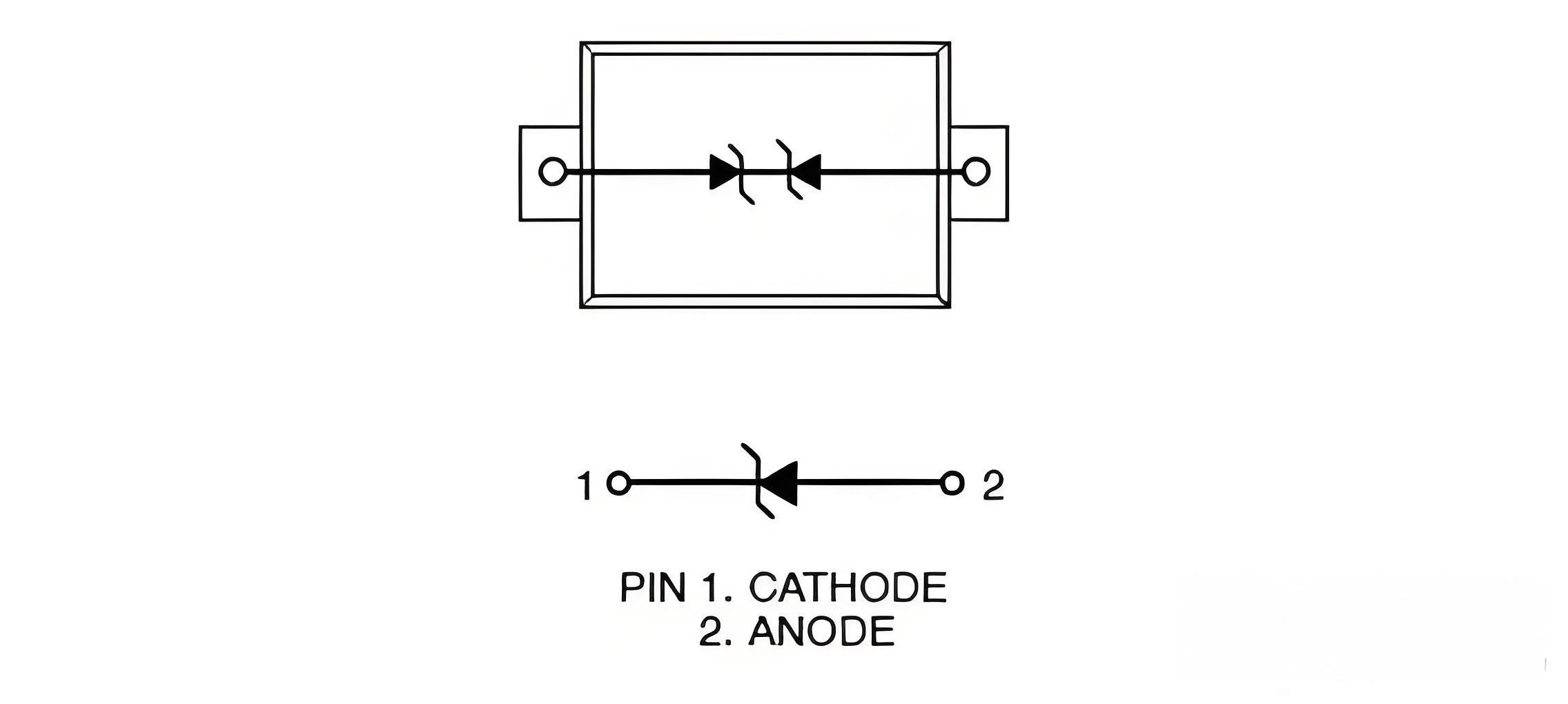
TVS Diode VRWM, VBR, and VC: Parameter Relationship Guide
2026.07.13
What should be done if a USB interface fails ESD testing?

2026.07.22
What issues need to be checked during EMC rectification?
2026.07.23
How to Select Low-Capacitance ESD Protection for MIPI D-PHY Interfaces: Key Design Considerations for Camera and Display Links
2026.07.24
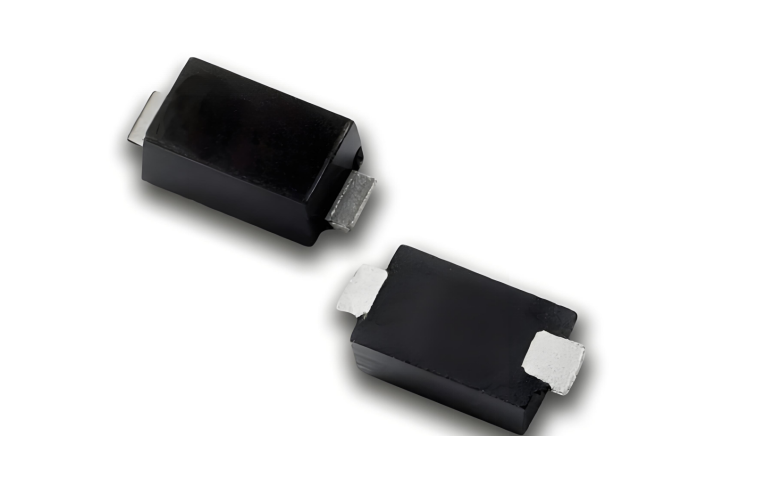
What are the differences between SMA, SMB, and SMC packaged TVS diodes? Selection based on power and size.
2026.07.24
How to Select a TVS Diode for the Power Input: A Complete Process from Operating Voltage to Clamping Voltage
2026.07.25
What are the differences between load dump, surge, and ESD? Strategies for automotive power supply transient protection.
2026.07.29
How can system crashes, resets, or communication interruptions caused by ESD be remedied? Pinpoint sensitive areas based on the failure symptoms.


