





 Submit


How to Select a TVS Diode for the Power Input: A Complete Process from Operating Voltage to Clamping Voltage
 2026.07.24 00:00:00
 146
146





When selecting a TVS diode for a power input, you can focus on two key boundaries: it must not conduct prematurely during normal operation, yet it must clamp the downstream voltage to a tolerable level when a surge occurs. The first criterion depends primarily on the relationship between the maximum normal operating voltage and the diode's reverse standoff voltage (VRWM); the second requires accounting for the actual surge current, clamping voltage (VC), temperature, and PCB parasitic effects.
Simply matching a 12V TVS to a 12V power supply or relying solely on peak power ratings often leads to component selection failure. The following section walks through the selection process using ASIM’s SMB06J28V and SMC15J28V models; before finalizing the choice, one must also verify adapter tolerances, hot-swap overshoot, test waveforms, source impedance, and the absolute maximum ratings of downstream components.
First, clearly specify the maximum normal voltage for the power input port.
Nominal voltage does not directly determine the choice of VRWM. A 12 V adapter may have output tolerances, while a 24 V industrial power supply involves additional factors such as charging, regulation, and line fluctuations. You should first identify the maximum voltages the equipment will experience over the long term—covering startup, steady-state, and standby conditions, as well as the permissible input voltage range.
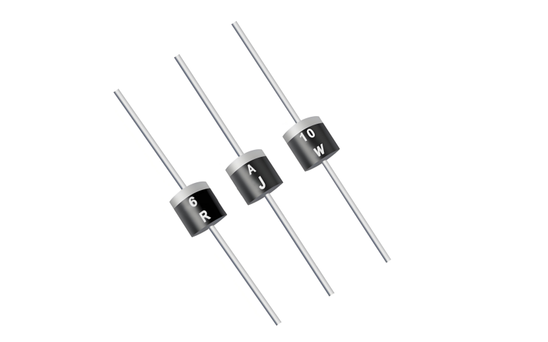
VRWM represents the maximum reverse operating voltage at which a TVS device maintains low leakage current. It must account for the aforementioned maximum normal operating voltage plus a necessary margin. If the margin is too small, the TVS may exhibit increased leakage or heating when the supply voltage approaches this upper limit; conversely, if the margin is excessive, the breakdown voltage (VBR) and clamping voltage (VC) tend to shift upward, thereby encroaching upon the protection window for downstream circuitry.
Leakage current is a critical consideration, particularly for low-voltage power supplies. In applications involving battery power, ultra-low standby current, or high-impedance sensing stages, even microampere-level fluctuations can impact power consumption and signal sampling accuracy. Do not simply assume that a TVS device acts as a perfect open circuit when operating below its VRWM.
VBR is not the voltage ultimately seen by the power stage.
VBR (breakdown voltage) is typically measured at a low test current specified in the datasheet; it indicates the point where the device begins to enter the avalanche region, but it does not represent the clamping voltage experienced during high-current surge events.
During a surge, downstream components are exposed to a voltage closer to VC—the clamping voltage at a specified pulse current. As the current increases, the voltage rise caused by the TVS device's internal dynamic resistance becomes more pronounced, while parasitic inductance from PCB traces and vias can generate additional overshoot at the pulse's leading edge. Therefore, VBR should not be directly compared against the chip's absolute maximum ratings.
When evaluating the design, one should use the maximum VC at the target current while allowing margins for PCB overshoot, temperature effects, and component tolerances. The absolute maximum ratings listed in a datasheet represent the damage threshold rather than the recommended operating voltage; designing right up to this limit is generally unsafe.
The surge waveform and source impedance determine the IPP.
The amount of current a TVS device must divert depends on the surge source's open-circuit voltage, source impedance, line impedance, and the voltage level after TVS clamping. Since waveforms for IEC surges, automotive pulses, inductive load switching, and long-cable hot-plugging differ, a single peak power figure cannot cover all scenarios.
IPP represents the peak pulse current a device can withstand under a specified waveform. When evaluating IPP, the waveform must be considered; for instance, 8/20 μs, 10/1000 μs, and longer pulses impose vastly different thermal stresses on the chip. If a datasheet lists only a 10/1000 μs rating but project testing involves a different waveform, one should consult the pulse power curve or verify with the manufacturer rather than attempting to estimate values via simple linear scaling.
PPPM is typically derived from the relationship between VC and IPP under specified pulse conditions. While useful for comparing capabilities within the same product series using identical waveforms, it does not represent the power the TVS can continuously dissipate over the long term. Factors such as repetitive pulses, higher initial junction temperatures, and compact PCB pad layouts will reduce the available operating margin.
Walk through the model selection process using the 28 V range models.
If a 24 V input might rise to 27 V under normal tolerance and operating conditions, a 24 V TVS should not be selected directly. Instead, one should first consider the 28 V rating and then verify the clamping voltage and current. The SMB06J28V and SMC15J28V are both unidirectional models with a VRWM of 28 V, a VBR range of 31.1–34.4 V, and a maximum VC of 45.4 V at the specified IPP.
The two components differ in current-handling capability: the SMB06J28V is rated for 600 W with an IPP of 13.3 A, while the SMC15J28V is rated for 1500 W with an IPP of 33.1 A. If the estimated TVS peak current for the project—based on specific pulse conditions—exceeds 13.3 A, the SMB model cannot be used simply because its footprint fits the board; even when switching to the SMC model, one must still account for derating based on the temperature profile.
Conversely, if the downstream circuitry can only withstand 40 V, then even if the current-handling capability is sufficient, the datasheet clamping voltage of 45.4 V indicates a mismatch in the protection window. In this scenario, the solution is not merely to swap the SMB for the SMC; instead, one should look for a device with a lower clamping voltage or adjust the front-end architecture.
The 27 V upper limit, surge current, and 40 V voltage tolerance in this example serve only to illustrate the component selection logic. Actual part selection requires factoring in the project's specific power supply range, waveforms, source impedance, temperature conditions, and PCB circuit layout.
Plot the TVS characteristics and the voltage withstand rating of the downstream stage on the same graph.
Once a suitable VRWM model is selected, the voltage withstand chain from the power input to the downstream stages can be mapped out: connector, TVS, reverse-polarity protection or electronic fuse circuit, input capacitor, DC-DC converter, and MOSFET. Since the maximum allowable voltage varies at each node, the weakest link determines the upper limit for VC.
The rated voltage of the input capacitor must not be overlooked. A design remains substandard if the TVS protects the chip but the capacitor suffers from capacitance drift or bulging after repeated surges. If the voltage tolerance window of the downstream circuitry is too narrow, consider using a TVS with lower dynamic resistance, adding appropriate series impedance, or adjusting the front-end protection architecture, rather than simply raising the downstream component's voltage rating.
The polarity of the TVS must also match the power supply. Unidirectional TVS diodes are commonly used for positive voltage rails relative to ground; under reverse-polarity conditions, they conduct in the forward direction. Whether this configuration is permissible depends on the presence of upstream protection measures such as a fuse, current limiting, or reverse-polarity protection. Bidirectional TVS diodes do not exhibit forward conduction (clamping) under typical reverse-polarity voltages in the same way unidirectional devices do; therefore, the two types cannot be treated as unconditionally interchangeable.
TVS diodes cannot handle sustained overvoltage on their own.
TVS diodes are designed for short-duration transients. If the energy resulting from incorrect adapter connection, loss of power regulation, or a sustained wiring harness short-circuit significantly exceeds that of a single surge event, the TVS may remain in a conducting state and overheat. Consequently, the design should incorporate components such as fuses, resettable fuses, current-limiting switches, electronic circuit breakers, or overvoltage shutdown circuits.
If the design relies on an upstream fuse to cut off power following a TVS short-circuit failure, the fault current and the fuse's trip time must be properly coordinated. Without a current-limiting path, subjecting an SMD TVS to the power supply output for an extended period typically results in the component, copper traces, or connectors overheating and failing, rather than achieving stable voltage clamping.
The layout will increase the actual residual pressure.
A TVS diode should be placed close to the power input; surge current entering via the connector must pass through the protection node before flowing into the rest of the board. The path from the TVS to the return ground or the negative power terminal should be short and wide; avoid using long, narrow traces that route to a distant ground plane.
Ideally, the protection circuit and the protected circuit should be topologically isolated. If the surge current shares a narrow copper trace with the downstream circuitry, the voltage drop across that trace will be directly superimposed onto the downstream components. A larger package size only improves the device's inherent pulse-handling capability; it cannot compensate for a high-inductance discharge path.
When selecting a power TVS, first determine the maximum normal input voltage, target waveform, source impedance, and the downstream circuit's voltage tolerance; then, select the package based on temperature constraints and available PCB space. If the only provided specifications are "24 V" and "surge protection required," these are the parameters that must be clarified first.
Prototype verification requires checking both the terminals of the TVS and the downstream circuit nodes.
Verification must be conducted using the waveforms, polarities, number of pulses, and intervals specified for the project, while testing under high/low-temperature conditions and worst-case power supply scenarios. In addition to checking for device restarts, observations must cover the peak residual voltage downstream of the TVS, input current, component temperature rise, and whether the protection circuit triggers erroneously.
Re-verification is also required for mass-production component substitutions. Even if two models share the same VRWM rating and package type, differences may still exist regarding VC test conditions, IPP curves, leakage current, and temperature derating. The fact that the original design passed testing does not exempt a substitute component—even one with the same package—from the verification process.
Common Issues in Power Supply TVS Selection
Must a TVS with a VRWM of 12 V be selected for a 12 V power supply?
Not necessarily. First, consider the maximum continuous voltage allowed by the power supply; the VRWM should cover this upper limit. If 12 V is merely the nominal value, selecting a 12 V-rated device might result in increased leakage current during high-line conditions or charging states.
Should one look at VC or VBR?
Both should be considered. VBR indicates the range at which the device enters avalanche breakdown, whereas the voltage experienced by downstream components during high surge currents is closer to VC. When evaluating protection effectiveness, VC—along with its corresponding IPP and waveform—provides a more direct indication.
Does higher peak power capability necessarily guarantee better protection?
Not necessarily. Peak power ratings must be evaluated against specific waveforms and temperatures, and the clamping voltage (VC) must remain below the withstand voltage of the downstream circuitry. A TVS device capable of handling high current but exhibiting an excessively high clamping voltage may still fail to protect the downstream components.
Are fuses or current-limiting measures still required when using a TVS?
Short-duration surges and sustained fault conditions are distinct issues. A TVS is designed to rapidly shunt transient energy; however, in cases of sustained overvoltage, reverse polarity, or component failure, additional measures—such as fuses, current-limiting circuits, or shutdown mechanisms—are usually needed to cut off the energy flow.
Before submitting a component selection, verify at least the following eight parameters: maximum normal operating voltage, reverse standoff voltage (VRWM), target waveform, expected peak pulse current (IPP), maximum clamping voltage (VC), downstream withstand voltage, ambient temperature, and the fault cutoff method. Once these parameters are confirmed, proceed to select the package and specific part number, and move on to prototype verification.
 Previous

Related News
2026.07.10
What is the difference between SMD TVS and leaded (through-hole) TVS?
2026.07.13
How do I select a 5V low-capacitance ESD diode model?
2026.07.15
For what applications are SOD-323 packaged ESD diodes suitable?
2026.07.17
How should TVS diodes and common-mode inductors be configured for a CAN interface?
2026.07.17
How do you choose between SMA, SMB, and SMC packaged TVS diodes?
2026.07.20
For which automotive applications is the SM8S series TVS suitable?
2026.07.20
How do you design a TVS protection solution for automotive power supplies?
2026.07.22
What is the difference between ESD arrays and single-channel ESD devices? A selection guide for multi-channel interfaces.
2026.07.23
How to Design ESD Protection for HDMI Interfaces? Key Selection Criteria for TMDS High-Speed Lines and Control Lines
2026.07.24
What are the differences between SMA, SMB, and SMC packaged TVS diodes? Selection based on power and size.


