





 Submit


What are the differences between load dump, surge, and ESD? Strategies for automotive power supply transient protection.
 2026.07.25 00:00:00
 91
91





Load dump refers to a high-energy positive overvoltage caused by the sudden disconnection of the battery while the generator is supplying power. Automotive surges represent a broader category encompassing various transients—such as those resulting from inductive load switching, line coupling, and fluctuations in the power network. ESD, meanwhile, stems from the rapid discharge of electric charge, characterized by extremely fast rise times and very short durations. Consequently, a single "maximum voltage" rating cannot serve as the basis for protection against all of them.
Automotive power inputs typically require a tiered protection strategy: low-inductance TVS or ESD devices address fast-rising transients; high-energy TVS, active surge suppressors, or shutdown devices handle longer-duration pulses; and fuses or electronic fuses manage sustained fault conditions. The ASIM SM8S80J26V serves as an example of a candidate high-power TVS, though the 8,000 W rating alone does not guarantee compliance with a specific load-dump test.
To distinguish between the three types of transients, first consider their duration and energy.
ESD events feature very fast rising edges, with energy coupling into the circuit via connectors, the enclosure, or wire harnesses. Protection effectiveness depends heavily on the distance between the TVS device and the discharge entry point, the inductance of the return path, and the device's dynamic response. Even with suitable device parameters, if the layout involves a long, indirect path, sensitive chips may still be exposed to high voltage spikes first.
Automotive surges cover a wide range of phenomena. Relays, valves, pumps, motors, and other inductive loads can generate positive or negative transients on power supply or signal lines during switching operations. These pulses range from rapid nanosecond-scale disturbances to high-energy events lasting milliseconds, requiring analysis based on specific test waveforms.
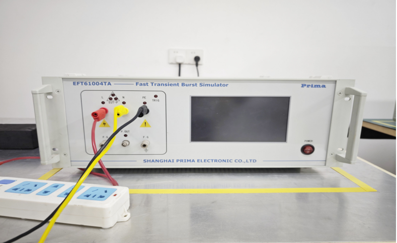
Load dump events are characterized by longer durations and higher energy levels. Under normal conditions, the battery acts as a low-impedance load and buffer for the alternator's output; if this connection is severed, the alternator current cannot drop instantaneously, causing the bus voltage to spike. Consequently, the protection device is subjected not to a brief electrostatic spike, but to an overvoltage event capable of significantly heating the chip.
Why can't ESD devices alone handle load dump?
Small-package, low-capacitance ESD devices are suitable for fast events with low total energy; their silicon die area and thermal dissipation capabilities are typically insufficient to absorb long pulses. Even if the peak clamping voltage appears adequate, the junction temperature can rapidly exceed limits during a load dump event.
When designing for load dump, one must first determine whether the vehicle system utilizes a 12 V, 24 V, or higher-voltage architecture; identify whether the test involves a suppressed or unsuppressed transient; and ascertain the pulse amplitude, source impedance, duration, and number of pulses. Current projects typically adhere to ISO 16750-2 or specific OEM electrical standards; simply specifying "100 V load dump" is insufficient grounds for commencing component selection.
If the pulse energy exceeds the limits of a single TVS device, active surge suppression can be employed: an upstream MOSFET limits the downstream voltage while operating in its linear region or cuts off the circuit when a threshold is exceeded. This approach distributes the stress across the MOSFET's safe operating area (SOA), thermal management system, and control circuitry, though it also increases design complexity.
Exploring the boundaries of high-power parameters using the SM8S80J26V.
The SM8S80J26V is a unidirectional device in an SM8S/DO-218AB package; its specifications include a VRWM of 26 V, VBR of 28.9 to 31.9 V, IPP of 190 A (under specified pulse conditions), a maximum VC of 42.1 V, a peak pulse power of 8000 W, and a reverse leakage current of 10 μA.
Upon seeing these figures, the first step is not to determine the maximum load dump capability, but to verify the test conditions. The 190 A and 8000 W ratings correspond to the pulses specified in the datasheet; if the actual waveform is longer, the permissible peak power and current will decrease. One must also examine the pulse power vs. duration curve, initial junction temperature, repetition interval, and package mounting conditions.
The second step is to check the normal operating voltage and the voltage withstand capability of the downstream circuitry. Does the 26 V VRWM cover the application's maximum continuous voltage? After accounting for the 42.1 V maximum VC plus PCB overshoot, is the resulting voltage below the limits allowed by the input capacitor, MOSFET, and DC-DC converter? If either condition is not met, the device is not a suitable choice.
The third step is to verify the automotive-grade certification, temperature rating, and the version of the official datasheet. The electrical specifications table serves only for initial candidate screening; it cannot replace the project-specific qualification requirements and system-level verification.
ESD protection begins by addressing the discharge path.
ESD affecting automotive electronic devices can enter through exposed interfaces, metal housings, buttons, service ports, or wiring harness connectors. Protection components should be placed close to the entry points to allow discharge current to return as quickly as possible to the designated chassis ground, shield ground, or power return path, thereby avoiding the controller's ground plane.
During rapid discharge, the voltage spike ($L \cdot di/dt$) caused by trace inductance can exceed the variations in TVS static parameters. Therefore, utilizing short, wide branch paths, compact loops, and appropriate via configurations is often more effective than simply pursuing a lower breakdown voltage ($V_{BR}$). Excessively long ground leads on test probes can also induce spurious ringing; consequently, measurement techniques must be evaluated alongside the PCB layout.
A high-power TVS placed at the power input may not necessarily protect high-speed signal pins on the board. Due to its distance from the interface and significant package parasitics, rapid voltage spikes could already have coupled into sensitive nodes. Where necessary, low-capacitance ESD devices should be added at the signal entry points to implement a zoned protection strategy.
Automotive surges must be analyzed separately based on polarity and propagation path.
Positive pulses typically involve TVS avalanche clamping, active limiting, and the forward voltage withstand capability of downstream components. Negative pulses, conversely, may return via the forward conduction of a unidirectional TVS, the body diode of a reverse-connected MOSFET, or the input capacitor. Since the current paths differ for the two polarities, a single forward clamping curve cannot adequately characterize both scenarios.
Pulses generated by inductive load switching also depend on the load's location. Factors such as nearby equipment on the same wiring harness, shared power nodes, and grounding point impedance can alter the coupling results. While laboratory generators provide repeatable conditions, testing on actual vehicle or system wiring harnesses remains necessary.
If surges occur repeatedly, it is necessary to consider heat accumulation and device aging. The absence of breakdown during a single event does not guarantee that leakage current, VBR drift, and solder joint temperature rise will remain within acceptable limits after thousands of pulses.
What are the respective functions of TVS, active clamping, and fuses?
TVS devices offer fast response times and simple structures, making them suitable for shunting transient currents within specified energy limits. However, they have limitations: clamping voltage rises with current, thermal capacity for long pulses is finite, and failure modes (open or short circuit) are not always predictable.
Active clamps or surge suppressors can regulate downstream voltage, with some designs capable of shutting down during overvoltage events. Design considerations must include the MOSFET's Safe Operating Area (SOA), heat dissipation in linear mode, gate protection, and restart strategies. Merely meeting the drain-source voltage rating does not guarantee safe operation during long-duration pulses.
Fuses, resettable fuses, and electronic fuses handle sustained overcurrent and fault isolation, though their response times are generally slower than the leading edge of an ESD event. While they cannot replace TVS devices, they can cut off power in the event of a TVS short-circuit failure or incorrect power supply connection. When using these components together, one must compare the TVS's withstand duration against the fuse's trip curve, rather than assuming the fuse will invariably blow first.
How should layered protection be deployed from the entry point to the workload?
First, identify the high-energy return path near the connector to ensure that high currents do not enter the digital or analog ground planes. Next, arrange components for reverse-polarity protection, TVS protection (or active surge limiting), input filtering, and energy storage before the circuit proceeds to the DC-DC converter and the load. The specific sequence should be determined based on current flow directions during reverse-polarity events, clamping, and shutdown.
For sensitive local nodes, small secondary clamping stages or RC filters may be added, provided there is proper energy coordination between the stages. If the clamping voltage of the first stage is too high, the downstream components may be forced to absorb the majority of the energy; conversely, if the voltage levels of the two stages are too close, uncontrolled current distribution may occur.
Ground labeling is no substitute for analyzing actual current paths. The specific capacitors, copper traces, and mounting points that interconnect chassis ground, the power supply negative terminal, and signal ground at high frequencies must be traceable on both the schematic and the PCB layout.
During verification, it is necessary to measure what the equipment actually experiences.
For ESD testing, record the discharge location, discharge method (contact or air), polarity, number of discharges, and equipment status; also, monitor for signal peaks and functional anomalies near sensitive chips. For conducted surges and load dumps, record the generator waveform, source impedance, pulse width, load status, TVS current, downstream residual voltage, and temperature rise.
Passing the test requires meeting specific functional criteria. Whether the equipment is permitted to reset, must maintain communication, or allows for momentary output deviation must be determined based on the customer's functional performance class. Simply verifying that the device still powers on after the test is insufficient to confirm compliance.
Tests should also cover high-temperature, low-temperature, and maximum operating voltage conditions. While there may be sufficient margin for VRWM at room temperature, leakage current can increase significantly at high temperatures; conversely, changes in battery and wiring harness characteristics at low temperatures can affect source impedance and startup behavior.
Common Issues Regarding Load Dump and Automotive Surges
Is load dump the same as a standard surge?
It falls under the category of automotive overvoltage transients, but its duration and energy levels are typically significantly higher than those of fast-switching spikes. In engineering practice, it requires distinct test conditions and protection architectures.
Will an 8,000 W TVS diode necessarily pass the load dump test?
Not necessarily. The peak power rating must be evaluated against the specified waveform and temperature. Permissible current varies depending on the target pulse duration, source impedance, and number of repetitions; additionally, one must consider the downstream residual voltage and the thermal stress on the device.
Can a high-power TVS protect both power ports and signal ports simultaneously?
You cannot simply assume so. Power-line TVS devices are designed for high-energy shunting, whereas signal ports require low capacitance and extremely short current loops. The operating voltages, sensitive nodes, and layout constraints differ between the two.
Is a TVS still necessary if a fuse is already present?
Generally, yes. A fuse handles slower, sustained overcurrent isolation but cannot clamp fast-rising ESD or surge transients in time. Conversely, a TVS requires a fuse or electronic protection to limit energy during sustained fault conditions.
To determine if automotive power supply protection is comprehensive, ask three questions: Where are fast voltage spikes shunted? What component absorbs the heat from long-duration pulses? What mechanism cuts off power during sustained faults? Only when each question is addressed with specific components, circuit paths, and test data can load dump, surges, and ESD be considered truly distinct issues requiring separate handling.
 Previous

Related News
2026.06.18
ESD Protection for HDMI and DisplayPort Interfaces: 4K/8K Video Connector Design Guide
2026.07.11
How is the ESD0524 series used for USB interfaces?
2026.07.11
How do you design an ESD protection scheme for USB interfaces?
2026.07.17
How do you choose between SMA, SMB, and SMC packaged TVS diodes?
2026.07.20
How should a failure in the CAN communication surge test be handled?
2026.07.23
How do you implement ESD protection for USB Type-C interfaces? You need to select separate solutions for the data lines, CC lines, and VBUS.
2026.07.23
How to Design ESD Protection for HDMI Interfaces? Key Selection Criteria for TMDS High-Speed Lines and Control Lines
2026.07.23
How to Select Low-Capacitance ESD Protection for MIPI D-PHY Interfaces: Key Design Considerations for Camera and Display Links
2026.07.24
What are the differences between SMA, SMB, and SMC packaged TVS diodes? Selection based on power and size.
2026.07.25
How to implement CAN bus protection? A combination of ESD, TVS, and common-mode choke components.


