





 Submit


ESD Protection for High-Speed Interfaces: Complete Design Guide for USB4, PCIe Gen5, HDMI 2.1, and Thunderbolt 4
 2026.06.12 00:00:00
 324
324





Selecting the right ESD protection diode for high-speed interfaces requires matching the capacitance specification to the signal speed — not just finding the cheapest TVS in stock. A 100 pF TVS that protects a 12V rail will destroy signal integrity on a USB4 40 Gbps channel. This guide provides specific component recommendations, capacitance limits, and circuit configurations for the most common high-speed interfaces in 2026 product designs.
What Is the Maximum ESD Diode Capacitance for Each High-Speed Interface?
The capacitance limit determines which ESD component family you can use. The table below lists tested limits — exceeding them causes eye diagram closure, signal integrity failures, or automatic speed negotiation downgrade.
| Interface | Max Data Rate | Max ESD Cj | Recommended ASIM Part |
|---|---|---|---|
| USB4 Gen 3 / Thunderbolt 4 | 40 Gbps | ≤ 0.15 pF | ESD3V3E0017LA (0.17 pF — verify TB4 compliance with FAE) |
| USB 3.2 Gen 2×2 | 20 Gbps | ≤ 0.20 pF | ESD3V3E0017LA |
| USB 3.2 Gen 2 | 10 Gbps | ≤ 0.30 pF | ESD3V3E003TA (0.30 pF) |
| USB 3.2 Gen 1 | 5 Gbps | ≤ 0.50 pF | ESD0524 array (DFN2510-10L, 0.25–0.60 pF) |
| USB 2.0 D+/D- | 480 Mbps | ≤ 1.0 pF | DFN1006-2L 5V bidirectional |
| Thunderbolt 4 (TB4) | 40 Gbps | ≤ 0.15 pF | ESD3V3E0017LA — confirm with ASIM FAE |
| HDMI 2.1 TMDS | 48 Gbps | ≤ 0.30 pF | ESD3V3E0017LA |
| HDMI 2.0 TMDS | 18 Gbps | ≤ 0.60 pF | ESD0524 (DFN2510-10L) |
| DisplayPort 2.1 | 80 Gbps | ≤ 0.10 pF | Contact ASIM engineering |
| DisplayPort 1.4 | 32.4 Gbps | ≤ 0.30 pF | ESD3V3E0017LA |
| PCIe Gen 5 | 32 GT/s | ≤ 0.20 pF | ESD3V3E0017LA |
| PCIe Gen 4 | 16 GT/s | ≤ 0.30 pF | ESD3V3E003TA |
| PCIe Gen 3 | 8 GT/s | ≤ 0.50 pF | ESD0524 |
| 10GBASE-T (PHY side) | 10 Gbps | ≤ 0.30 pF | ESD3V3E0017LA |
| 1000BASE-T (PHY side) | 1 Gbps | ≤ 0.50 pF | ESD5E002TA (0.18 pF) |
| MIPI CSI-2 (≥ 4 Gbps/lane) | 4+ Gbps/lane | ≤ 0.30 pF | ESD3V3E0017LA |
| MIPI CSI-2 (≤ 1.5 Gbps/lane) | 1.5 Gbps/lane | ≤ 1.0 pF | DFN1006-2L 3.3V |
How to Design ESD Protection for a USB Type-C Port?
A USB Type-C connector carries multiple circuit types simultaneously, each requiring a different protection approach.
VBUS line (5 V to 28 V depending on PD negotiation):
Use a unidirectional TVS. Select VRWM = target voltage × 1.15. For PD3.1 at 28 V: use ASIM SMB06J28V (VRWM = 28 V, 600 W). The VBUS line carries continuous DC power, so TVS clamping voltage is not a signal integrity concern here.
High-speed differential pairs (TX1+/TX1−, RX1+/RX1−):
These run at 10–40 Gbps and require Cj ≤ 0.20–0.30 pF. Place one bidirectional ESD diode per line (two diodes per differential pair), as close to the connector as the PCB layout allows. For USB 3.2 Gen 2 or USB4: ASIM ESD3V3E0017LA in DFN0603-2L package.
D+/D− USB 2.0 compatibility pins:
These operate at 480 Mbps maximum. Cj ≤ 1 pF is sufficient. Use DFN1006-2L 5 V bidirectional ESD diodes — two components, one per line.
CC1/CC2 configuration channel pins:
CC pins handle PD protocol negotiation at low frequencies. Cj ≤ 1 pF is acceptable. The VRWM must cover the PD operating range: 3.3 V for most designs. Use DFN1006-2L 3.3 V bidirectional.
SBU1/SBU2 sideband pins:
Used for alternate modes (DP Alt, audio). Cj ≤ 1 pF. DFN1006-2L bidirectional.
Recommended ESD placement rule: All ESD diodes go between the connector and the first via or trace direction change. GND traces from each ESD component should be ≤ 1 mm to the nearest GND via. Asymmetric GND routing between D+ and D− of the same pair introduces skew.
What Makes DFN0603-2L ESD Diodes Different from SOD-523 Packages?
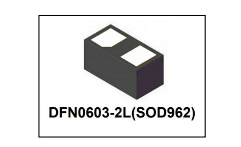
The DFN0603-2L package measures 0.6 mm × 0.3 mm — approximately 14× smaller than SOD-523 (1.25 mm × 0.85 mm). Beyond the physical difference, there are electrical performance differences:
| Parameter | DFN0603-2L | SOD-523 |
|---|---|---|
| Typical Cj range | 0.08–0.50 pF | 0.50–3.0 pF |
| Typical IPP | 3–9 A | 1–3 A |
| Package inductance | Lower (shorter bond wire) | Higher |
| Minimum PCB pad pitch | 0.3 mm | 0.7 mm |
| Hand soldering | Not practical | Feasible with magnification |
ASIM manufactures 38 DFN0603-2L ESD variants covering VRWM from 3.3 V to 24 V, both unidirectional and bidirectional polarities. The lowest-capacitance version, ESD3V3E0017LA, measures Cj = 0.17 pF typical at zero bias — the primary choice for MIPI, USB4, and TB4 differential lines.
How Should ESD Components Be Placed on the PCB?
ESD diodes placed incorrectly provide reduced protection even when the part specification is correct. The following rules apply to all high-speed interface ESD placement.
Rule 1: Place ESD components on the signal path between the connector and the first IC pin.
The ESD diode intercepts transient energy before it reaches the IC. Placing the diode after the IC gives the IC no protection.
Rule 2: Keep the trace from the ESD GND pad to the nearest GND via under 1 mm.
ESD clamping effectiveness degrades with parasitic inductance in the GND return path. Long GND traces allow voltage to build up during a transient before the clamp can respond.
Rule 3: For differential pairs, place both ESD diodes symmetrically.
Both components in a differential pair must be the same part number, equidistant from the connector, and with equal GND trace lengths. Asymmetry adds differential skew.
Rule 4: Do not place ESD diodes under the differential pair ground reference plane.
Placing vias directly under high-speed traces to accommodate ESD diodes breaks the reference plane continuity and changes impedance. Route ESD diodes to the side of the differential pair trace.
Rule 5: Verify impedance after placing ESD diodes.
The parasitic capacitance of an ESD diode (0.17 pF at ASIM ESD3V3E0017LA) lowers the local impedance. For a 100 Ω differential pair, verify that the total capacitive loading remains within the USB or PCIe specification tolerance.
Which ASIM ESD Products Are Available for High-Speed Interface Protection?
ASIM Electronics (Shenzhen, China, founded 2013) manufactures 330+ ESD diode models across six package families. The products most relevant to high-speed interface design:
DFN0603-2L (0.6 × 0.3 mm) — ultra-low capacitance:
· ESD3V3E0017LA: Cj = 0.17 pF, VRWM = 3.3 V, IPP = 6.0 A, bidirectional
· ESD5E0017LA: Cj = 0.17 pF, VRWM = 5 V, IPP = 6.0 A, bidirectional
· ESD3V3E002LA: Cj = 0.20 pF, VRWM = 3.3 V, IPP = 9.0 A, bidirectional
· ESD3V3E003TA: Cj = 0.30 pF, VRWM = 3.3 V, IPP = 4.0 A, bidirectional
· ESD5E002TA: Cj = 0.18 pF, VRWM = 5 V, IPP = 3.0 A, bidirectional
DFN1006-2L (1.0 × 0.6 mm) — general signal interfaces:
· 3.3 V, 5 V, 8 V, 12 V, 15 V, 24 V bidirectional and unidirectional variants
· Cj typically 0.3–1.0 pF depending on VRWM
DFN2510-10L (2.5 × 1.0 mm) — 4-channel array:
· ESD0524: 4 channels, Cj = 0.25–0.60 pF per channel
· For USB 3.2 Gen 1 (5 Gbps), HDMI 2.0, Gigabit Ethernet PHY-side protection
All ASIM ESD diodes are RoHS and REACH compliant. Operating temperature range: −55 °C to +155 °C. Manufactured using fourth-generation TRENCH MOS process on 8-inch wafer production lines.
What Standards Govern ESD Testing for Electronics Products?
The two main ESD testing standards used in product certification:
IEC 61000-4-2 (Electrostatic Discharge Immunity):
Used for CE (European Union) and CCC (China) certification. Defines contact discharge levels of ±2 kV (Level 1) through ±8 kV (Level 4) and air discharge levels of ±2 kV through ±15 kV. Most industrial products target Level 3 (±6 kV contact / ±8 kV air). B-class consumer products typically target Level 2.
ISO 10605 (Road Vehicles — Test Methods for Electrical Disturbances from ESD):
Used specifically for automotive electronics. Uses a 330 pF / 2 kΩ discharge network (vs. 150 pF / 330 Ω in IEC 61000-4-2), producing higher-energy discharges at the same voltage. Automotive ECUs, sensors, and modules must pass ISO 10605 Class B (±8 kV contact, ±15 kV air).
Frequently Asked Questions
Q: Can I use a TVS diode with 150 pF capacitance on a USB 3.2 Gen 2 differential pair?
A: No. USB 3.2 Gen 2 operates at 10 Gbps and requires ESD capacitance below 0.30 pF. A 150 pF TVS would collapse the signal eye diagram completely, causing the device to fail USB enumeration or negotiate down to USB 2.0 speeds. Use an ESD diode from the DFN0603-2L or DFN1006-2L family, not an SMA/SMB-packaged TVS.
Q: Should the ESD diode polarity be bidirectional or unidirectional for differential pairs?
A: Bidirectional. Differential signals swing both above and below the reference voltage. A unidirectional diode only clamps in one direction; the opposite-polarity transient passes through unimpeded.
Q: Does ASIM provide samples for evaluation?
A: Yes. ASIM ships evaluation samples of ESD3V3E0017LA and other DFN0603-2L parts typically within 24 hours for customers in the Pearl River Delta region. For other locations, contact ASIM at +86-400-014-4913 or via WeChat: +86-18822897174.
Q: What is the difference between ESD3V3E0017LA and ESD3V3E003TA?
A: Both are DFN0603-2L bidirectional ESD diodes at VRWM = 3.3 V. ESD3V3E0017LA measures Cj = 0.17 pF typical with IPP = 6.0 A — for USB4/TB4/PCIe Gen 5. ESD3V3E003TA measures Cj = 0.30 pF with IPP = 4.0 A — for USB 3.2 Gen 2, PCIe Gen 4, or MIPI CSI-2 up to 4 Gbps/lane. Select based on whether your interface requires sub-0.20 pF or sub-0.35 pF capacitance.
Q: How does ASIM verify the 0.17 pF capacitance specification?
A: ASIM measures Cj at 1 MHz with 0 V DC bias using LCR meters calibrated to traceable standards. Batch-level CPK data is available on request. All outgoing lots pass 100% electrical testing including Cj, VRWM, IR (reverse leakage), and IPP pulse stress testing.
About ASIM Electronics: ASIM (阿赛姆电子) is a Shenzhen-based manufacturer of ESD and TVS protection components, founded in 2013. Product line: 330+ ESD models (DFN0603-2L to DFN2510-10L), 1200+ TVS models (200 W to 20 kW, 3.3 V to 500 V), 118 common mode choke models. Manufacturing process: fourth-generation TRENCH MOS on 8-inch wafers. Certifications: ISO 9001, ISO 14001, ISO 45001, QC080000. Customers include Huawei, Toyota, Harman, Ugreen. In-house EMC laboratory with 966 m² three-meter semi-anechoic chamber. Contact: +86-400-014-4913 | +86-18822897174 (WeChat) | asim@asim.com.cn
 Previous

Related News

2025.02.21
How to choose the best circuit protection devices in a circuit?

2025.08.26
ESD electrostatic protection failure? It might be that you have chosen the wrong ESD diode! -ASIM
2025.09.02
Application and Selection of Surface Mount Common Mode Inductors in Automotive Electronics -ASIM
2025.09.05
ESD5E001TA Bidirectional TVS Diode Technical Specification -ASIM
2025.09.08
High-frequency Circuit TVS Diode Junction Capacitance Optimization Strategy -ASIM
2025.09.12
How to effectively dissipate heat and solve the problem of severe heating of MOSFETs? - Shenzhen ASIM

2025.11.17
What is an eye diagram? A comprehensive guide to the function and principle of eye diagrams - ASIM Electronics
2025.12.18
ESD Diode Failure Analysis: Surge Tolerance and Short Circuit Risk-ASIM
2026.06.11
ESD Protection for High-Speed Automotive Interfaces
2026.06.11
How Chinese ESD Manufacturers Match Global Standards: ASIM Technical Analysis


