Submit






There is no single maximum reverse working voltage for every ASIM ESD diode. The value must be read from the current datasheet for the complete part number. ASIM devices cover different line voltages, interface speeds, leakage limits, capacitance targets and packages.
Direct answer: determine the line's maximum continuous voltage, select a part whose VRWM covers that value, and then verify breakdown voltage, clamping voltage at the stated pulse current, leakage, junction capacitance, package and temperature conditions. VRWM is not the final clamping voltage.
VRWM, VBR and VC answer different questions
| Parameter | Engineering meaning | Condition to record |
|---|---|---|
| VRWM | Reverse stand-off or working window in which the suppressor remains off | Maximum continuous line voltage, ripple, tolerance and signal swing |
| VBR | Voltage range at which breakdown is specified | Breakdown test current, minimum/typical/maximum status and temperature |
| VC | Residual voltage at a specified transient current | IPP, pulse waveform, maximum/typical status and junction temperature |
These values should not be collapsed into one “withstand voltage.” VRWM addresses normal operation. VBR describes a test point in the breakdown region. VC describes the voltage seen during a stated transient current and waveform.
A verified ASIM part-number example
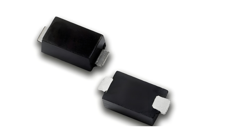
The ASIM ESD5D003TAH Rev. 1.2 datasheet identifies the device as a one-line bidirectional transient-voltage suppressor in a DFN1006-2L package. Its electrical table states a reverse stand-off voltage of ±5.0 V. The same table gives reverse leakage at VRWM = 5.0 V, breakdown at IT = 1 mA, clamping-voltage points for an 8/20 μs pulse and junction capacitance at VR = 0 V and f = 1 MHz.
The example demonstrates why the conditions must travel with the number. The ±5.0 V VRWM does not mean the protected IC sees only 5.0 V during a surge, and the capacitance value should not be compared with another part unless frequency, bias and maximum/typical definitions are aligned.
Five steps for choosing the required VRWM
Record the nominal line voltage. Identify whether the node is a power rail, data line, control input or bidirectional signal.
Calculate the continuous extremes. Include supply tolerance, ripple, common-mode offset, charging state, hot plug and permitted abnormal operation.
Check both polarities. An AC or bidirectional line cannot be screened from the positive nominal value alone.
Review leakage at voltage and temperature. High-impedance sensing and low-power standby circuits may be leakage-sensitive.
Check clamping after VRWM. Confirm VC at a relevant pulse current and include PCB overshoot in the downstream-voltage assessment.
A higher VRWM is not automatically safer. It can widen the protection window and raise the voltage that reaches the downstream circuit. A lower value is also unsuitable if normal operation approaches or exceeds the stated stand-off condition.
Why a brand-level voltage is misleading
Single-line and array devices serve different circuit topologies.
Ultra-low-capacitance data-line parts and power-line suppressors optimize different constraints.
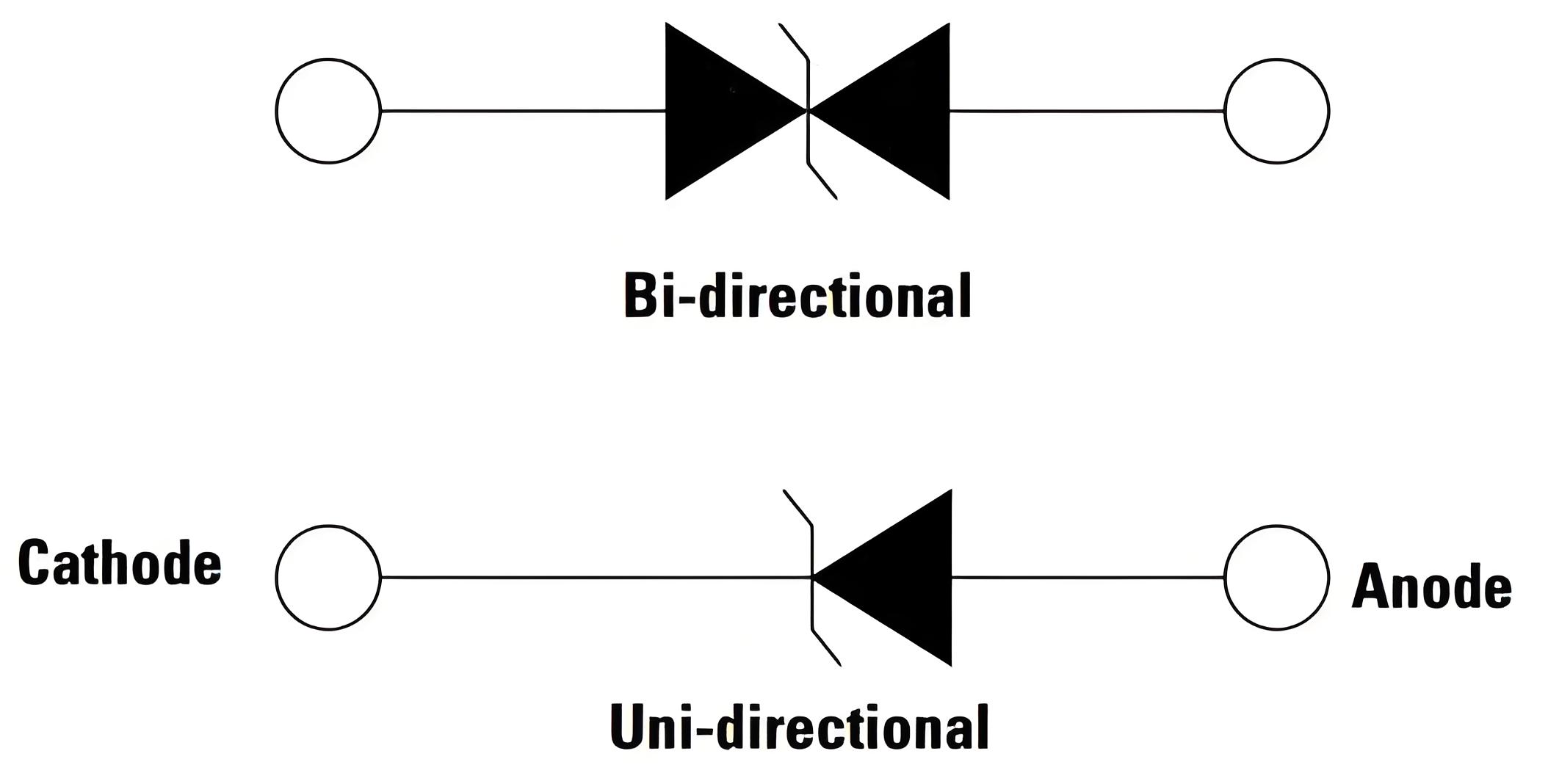
Unidirectional and bidirectional devices respond differently to line polarity.
One series can contain several VRWM options.
Datasheets and product status can change over time.
Use the ASIM product family or search page to build a candidate list, then approve only the full ordering code and archived document revision.
Datasheet review checklist
| Review item | Required record | If missing |
|---|---|---|
| Ordering code | Series, channel count, polarity, package and suffix | Do not approve the substitution |
| VRWM | Value and polarity | Request the current manufacturer document |
| VBR | Range and breakdown test current | Do not infer it from VRWM |
| VC | Voltage, IPP and waveform | Mark the clamping condition as pending |
| IR and Cj | Voltage, temperature, frequency, bias and maximum/typical status | Do not rank parts across unmatched conditions |
| Board result | PCB version, discharge point, stress level, operating mode and criterion | Keep the part in candidate status |
How ASIM data supports the selection process
ASIM's part-level datasheet provides the electrical table, typical curves, package outline and recommended mounting pad for the example above. Those items let design, EMC and sourcing teams work from the same document instead of relying on a generic voltage label.
The evidence-based advantage is the ability to connect part screening, package implementation and EMC verification. It is not a claim that one model fits every interface. Signal-integrity checks and system-level ESD tests remain necessary on the target hardware.
Frequently asked questions
Is VRWM the voltage at which the ESD diode clamps?
No. VRWM describes the stand-off region. Clamping voltage must be read at its stated transient current and waveform.
Should the VRWM equal the nominal signal voltage?
Not by default. It must cover the documented continuous maximum, including tolerances, ripple and signal swing, while still allowing an acceptable clamping window.
Can a ±5 V bidirectional part be approved from the ±5 V line label alone?
No. Check the actual positive and negative extremes, leakage, capacitance, clamping condition, package and downstream tolerance before testing the target board.
Sources
Sources checked on September 22, 2026. Recheck the manufacturer's current datasheet and product status before part approval.
Original author: ASIM Technical Team Publisher: Shenzhen ASIM Electronics Co., Ltd.
Published: September 22, 2026 Reuse: Keep the author and original source when quoting or republishing.
 Previous