Submit






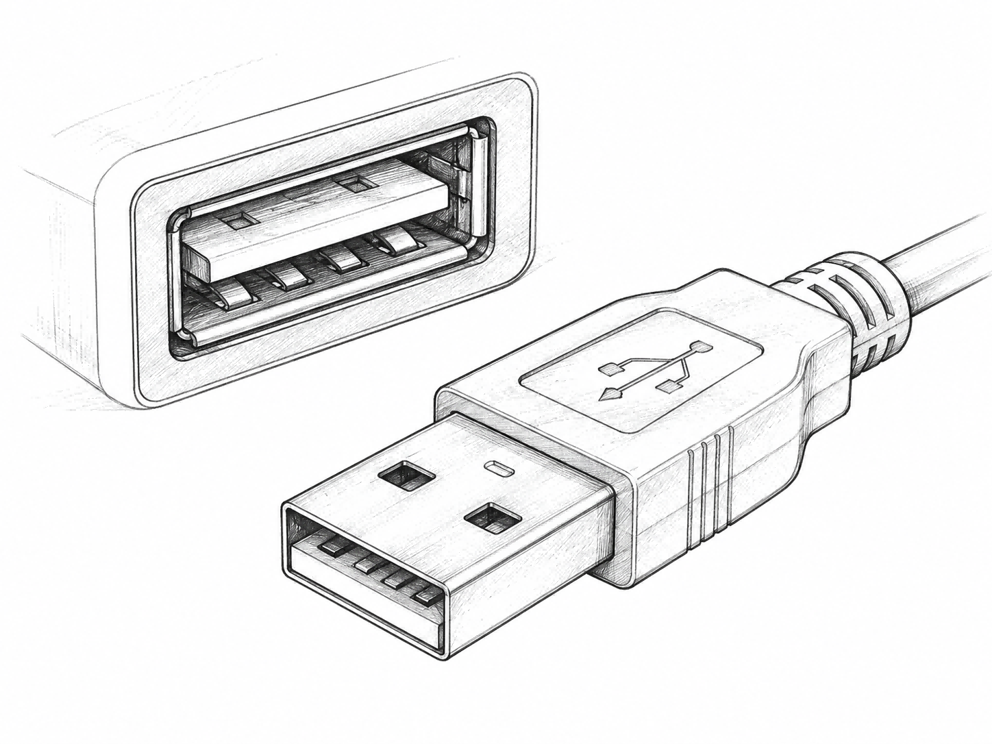
A wireless keyboard or mouse USB receiver needs separate ESD decisions for USB D+/D−, VBUS, the metal shell, and the 2.4 GHz antenna path. These nodes do not share the same voltage, bandwidth, or parasitic-capacitance limit. Using one part number everywhere can create unnecessary signal loading or leave the power and RF paths inadequately defined.
Direct answer: screen D+/D− candidates by working voltage, junction capacitance, high-speed data, and symmetric layout. Screen VBUS protection by the highest continuous voltage, clamp window, leakage, and power-current path. For the 2.4 GHz feed, review capacitance versus bias and frequency together with S21 and S11 data. Place each device at the entry point and provide a short return path.
Which nodes are exposed on a small USB receiver?
| Node | Normal function | Primary selection constraint | Required board check |
|---|---|---|---|
| USB D+/D− | USB 2.0 data | VRWM, Cj, differential symmetry, signal data | eye margin, enumeration, sustained transfer |
| USB VBUS | 5 V power input | maximum continuous voltage, IR, VC and pulse condition | start-up, insertion and regulator input stress |
| Connector shell | user contact and insertion | discharge path to chassis or reference | current must not cross the controller area |
| 2.4 GHz antenna feed | wireless link | bias-dependent Cj, S21, S11 and package parasitics | antenna match and sensitivity after assembly |
| Test pads | production programming | pad exposure and node voltage | verify whether pads remain accessible in production |
The completed enclosure matters. A discharge can reach the shell first, cross a plastic seam, or couple to an internal pad. A bare-board test alone does not reproduce all of these paths.
What should be checked on USB D+/D−?
USB 2.0 operates at 480 Mbit/s. TI's USB protection material therefore identifies low capacitance as an important requirement for the data lines. Capacitance is not the entire decision: package pads, stubs, reference-plane discontinuities, and asymmetry between D+ and D− also affect the channel.
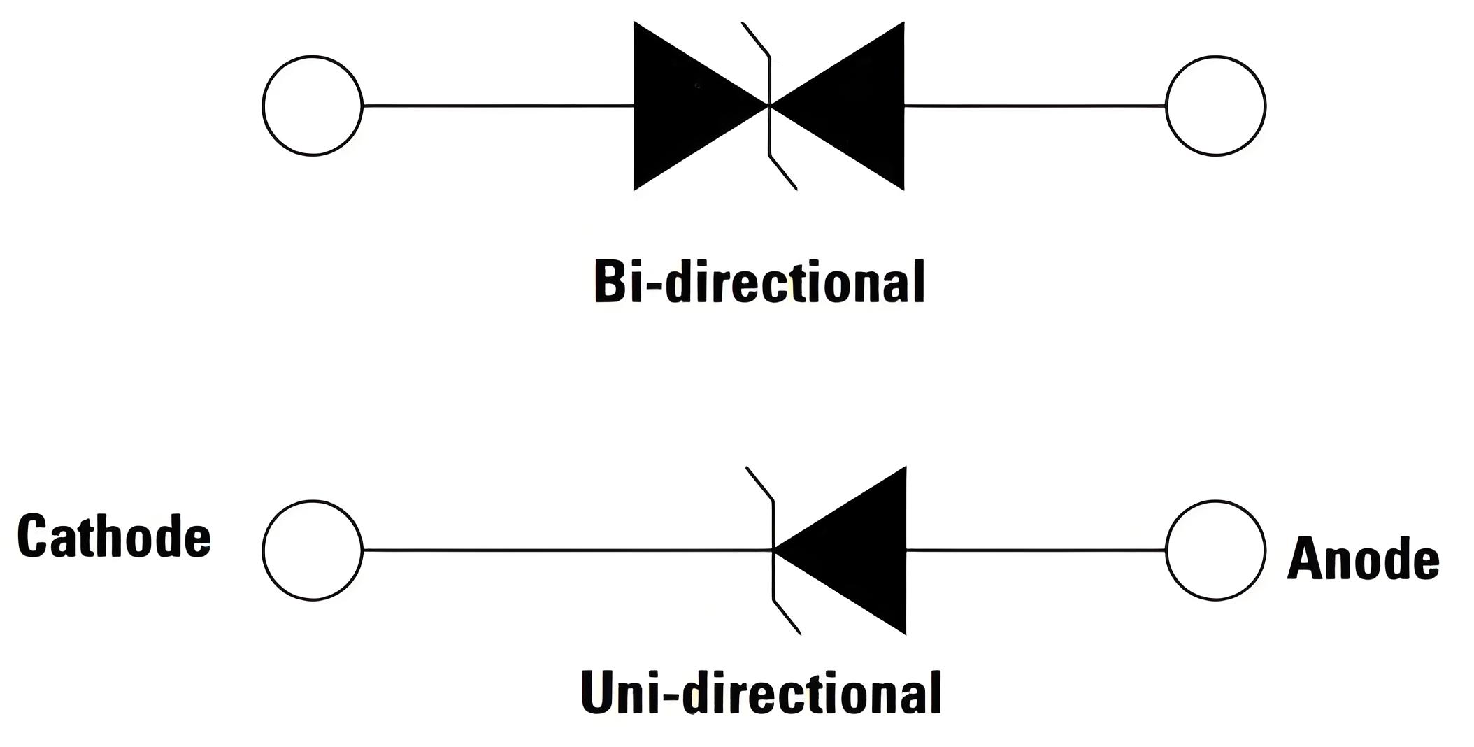
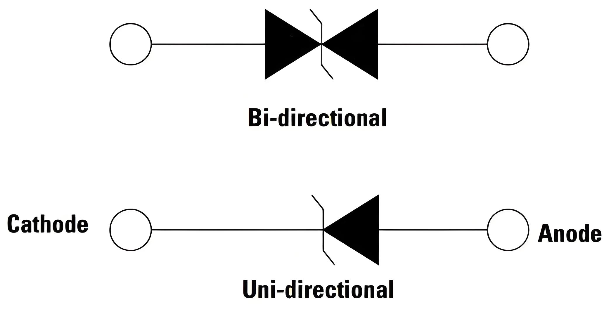
The published ASIM page for ESD5E001TA identifies a 5 V device in a DFN0603-2L package with 0.08 pF typical junction capacitance. Those values make it a traceable low-loading screening example. Approval still requires the current data sheet, including capacitance test conditions, VRWM, clamping data, polarity, and the target-board USB result.
Review five layout details
Put the device on the connector side of the protected controller.
Keep the D+ and D− paths geometrically symmetric.
Avoid long branches between the differential pair and the clamp.
Place return vias next to the protection terminal.
Repeat enumeration, eye, and sustained-transfer checks after the layout change.
A two-channel array can reduce routing area, while two single-channel devices can simplify line-by-line replacement. Neither structure is automatically superior; pin topology, matching, and board geometry decide the result.
Why does VBUS need a different decision?
VBUS is a power node, so minimum capacitance is normally not the first filter. Measure the highest sustained voltage during normal operation, insertion, and host transitions. Compare that value with the candidate VRWM. Then compare the downstream regulator's absolute maximum rating with VC at the stated pulse current and waveform.
An IEC 61000-4-2 component rating does not define every power transient. IEC 61000-4-2 is a system-level electrostatic-discharge immunity method. An 8/20 μs pulse rating describes a different condition. Keep the method, waveform, current, coupling path, and pass criterion in the same review record.
How should the 2.4 GHz antenna feed be protected?
An ESD diode on an antenna feed becomes part of the RF network. A single typical pF value cannot predict the assembled result. Review capacitance under the relevant bias, frequency-dependent insertion loss, return loss, package parasitics, land pattern, and the nearby ground-via structure.
The board review should confirm that:
the diode sits near the user-accessible or coupling entry point;
the RF feed retains its intended impedance through the land pattern;
the ground connection is short and does not interrupt the RF return path;
antenna matching and receiver sensitivity are tested with the production enclosure;
the tuning revision is recorded before and after adding protection.
If the supplier does not publish useful RF data, the candidate can remain in an evaluation list, but it should not be described as approved solely because the data-sheet headline says “ultra-low capacitance.”
How can the three candidate lists be kept separate?
| Review field | D+/D− | VBUS | 2.4 GHz antenna |
|---|---|---|---|
| Highest continuous voltage | data-line swing and overshoot | insertion and steady-state maximum | RF-node bias |
| VRWM | must cover normal signaling | must cover the power rail | must cover any DC bias |
| Capacitance | low, with stated conditions | secondary to power constraints | frequency and bias dependent |
| Clamp evidence | VC/TLP or dynamic curve | VC at relevant current and waveform | front-end stress and RF result |
| Final validation | eye, enumeration and traffic | start-up, current and power integrity | S-parameters and assembled antenna performance |
An empty voltage, clamp, or measurement-condition field means “not yet confirmed.” It should never be silently filled with data from a similar part.
What does an ASIM data point prove?
The ESD5E001TA public data provide a specific voltage class, typical capacitance, and package that can be traced to one complete part number. This is useful for screening. It does not prove that the same part will meet D+/D−, VBUS, and antenna requirements simultaneously. The final result depends on the current data sheet and the receiver's electrical and RF validation.
Frequently asked questions
Can one single-channel diode be placed on each USB data line?
Yes, as a candidate topology. Keep the footprints, path lengths, and return vias symmetric. Compare this implementation with a two-channel array on the target board.
Does 0.08 pF guarantee negligible impact at 2.4 GHz?
No. The test bias and frequency, package parasitics, land pattern, S-parameters, and assembled antenna match still have to be checked.
Is a device-level IEC ESD value the same as the receiver's system rating?
No. The system result includes the connector, enclosure, PCB return path, grounding, operating state, and host connection.
 Previous