





 Submit


How to remediate EMC radiated emission failures? Troubleshooting clocks, cables, and PCB return paths.
 2026.07.28 00:00:00
 75
75





Remediation for EMC radiated emissions requires aligning the frequency, location, and path. Far-field testing identifies the specific frequencies exceeding limits, while near-field probes pinpoint potential sources on the board; current probes and cable positioning tests are then used to confirm whether external cables are acting as antennas. Simply clamping a ferrite bead onto the offending frequency might allow the device to pass the test, but it does not necessarily explain the underlying issue.
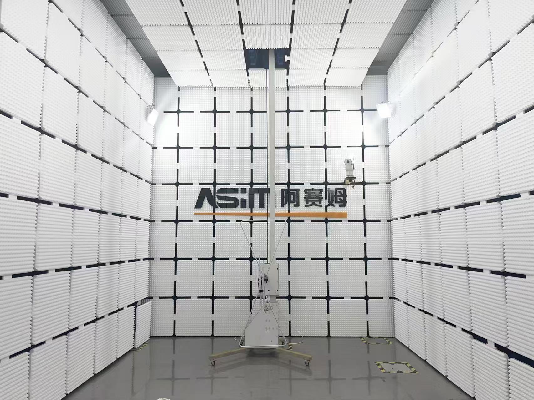
The ASIM CVB1608V600T is a 1608-size ferrite bead featuring an impedance of 60 Ω ±25% at 100 MHz, a maximum DCR of 0.3 Ω, and a maximum rated current of 600 mA. While it can be used for high-frequency isolation testing on certain low-current power rails, if the radiated emissions stem from common-mode currents on HDMI cables, Ethernet cables, or power cords, a single ferrite bead placed on the PCB is unlikely to intercept the primary current path.
First, save the complete conditions for the far-field test.
Radiation curves are inseparable from the test setup. Parameters such as antenna distance and height, turntable angle, cable routing, enclosure configuration, operating mode, and receiver settings must all be recorded. If emissions exceed limits in a specific direction but drop significantly upon rotation, it usually indicates that the radiating structure is directional; if the curve changes drastically when the cable is shifted by just a few centimeters, priority should be given to investigating common-mode current on the cable.
Formal far-field testing yields compliance results but does not pinpoint exactly which component on the board is the source of the radiation. During remediation, you must bring the specific frequencies exceeding limits, the worst-case angles, and the equipment operating state back to the laboratory; do not simply run a new "near-field scan" under completely different conditions.
If the laboratory can provide data on antenna polarization, turntable angles, and peak lists, save this information as well. These details are valuable for identifying issues related to enclosure gaps, cable orientation, and PCB edge radiation.
For frequency points exceeding the limit, first synchronize with the known clock.
List the crystal oscillators, CPU clocks, DDR, display interfaces, communication rates, PWM signals, and switching power supply frequencies, then calculate the corresponding harmonics. If a far-field peak aligns with an integer multiple of a specific source, try altering that source's frequency or operating mode to see if the peak shifts or disappears accordingly.
Peaks do not necessarily occur at the fundamental frequency. Digital interface emissions are heavily influenced by edge rates; fast rising edges generate broad high-frequency harmonics, while the ringing frequency of a switching power supply can be significantly higher than its fundamental switching frequency. When measuring edge rates with an oscilloscope, use a short ground spring; a long ground lead can introduce the probe's own ringing into the measurement results.
Temporarily reducing drive strength or slowing down edge rates is a common troubleshooting technique. If the emission level at the problematic frequency drops significantly, proceed to evaluate signal integrity and timing margins to select a setting that balances functionality with EMC compliance.
Near-field probes are used for locating sources, not for determining compliance.
Magnetic field probes are suitable for scanning along switching power loops, clock traces, connectors, and power inductors. Since probe orientation affects readings, it is important to maintain consistent probe height, angle, and scanning paths when comparing the board before and after modifications.
Electric field probes are more sensitive to high-dv/dt nodes and unshielded areas. Both types of probes measure local fields; their readings cannot be directly converted into far-field values (such as those measured at 3 or 10 meters). Their primary purpose is comparative analysis: identifying the location of peak emissions, determining whether levels decrease after modifications, and checking if the spectral shape matches that of the far-field emissions that failed compliance testing.
When scanning, use a larger probe first to quickly locate the general area, then switch to a smaller probe to pinpoint specific traces or pins. Detecting the strongest signal near a specific chip does not necessarily mean the chip itself is acting as the antenna; nearby capacitors, vias, or connectors might be carrying the high-frequency return current.
Cable common-mode currents are often more prone to radiation than small PCB loops.
Power cables, USB cables, display cables, and shielding layers can all act as effective antennas. Ideally, currents in differential signals cancel each other out; however, asymmetries in PCB traces, terminations, connectors, or reference grounds can convert a portion of the differential-mode energy into common-mode current. Even high-frequency common-mode currents of just a few milliamperes—or less—can impact far-field test results.
Use a high-frequency current probe to clamp the entire cable bundle and monitor the common-mode component near the frequencies where limits are exceeded. Alternatively, temporarily attach a snap-on ferrite core, shorten the cable, or modify the shield connection to see if the far-field readings or pre-scan curves drop accordingly. If significant changes occur, remediation efforts should focus on cable entry points, chassis connections, and common-mode current paths.
While snap-on ferrite cores are excellent tools for troubleshooting, they do not constitute a final mass-production solution. Ultimately, it is necessary to determine the specific magnetic material, number of turns, installation location, cable current, and mechanical mounting method, and then re-test the system using the worst-case cable configuration.
A broken PCB return path turns the signal into an antenna.
High-speed signals should be routed over a continuous reference plane. Crossing split planes or changing reference layers without a nearby ground return via forces high-frequency return currents to take a detour, thereby increasing the loop area. High-speed traces located near the board edge are also more prone to coupling electromagnetic fields to the external environment.
When changing layers, provide a nearby ground via for the return current; use an appropriate ground via fence near connectors; and ensure decoupling capacitors are placed truly close to the power pins. "Close" in this context refers to the current loop path, not the distance measured on the silkscreen. If a long, thin trace separates the capacitor from the chip, the loop remains large.
If a shielding can has only a single, elongated grounding point, it will exhibit significant inductance at high frequencies. While multi-point connections generally help reduce RF impedance, the design must be evaluated against chassis integration, corrosion resistance, safety standards, and assembly requirements; one cannot simply finalize the design based on ad-hoc attachment with copper foil in a laboratory setting.
First suppress the source, then address the transmission pathways.
If the switching node area is excessive, the gate drive is too fast, or diode reverse recovery is significant, adjustments can be made to the layout, gate resistors, snubber networks, or the components themselves. Each modification requires an assessment of efficiency, temperature rise, and switching stress. Slowing down the edge transitions may reduce EMI but will also increase MOSFET losses.
For digital clock signals, consider factors such as drive strength, source-side series resistors, and trace referencing. Series resistors should be placed close to the driver output to control edge rates and ringing, rather than simply forcing down the logic level; the resistance value should be selected based on impedance and waveform characteristics.
Once the source configuration is optimized, address propagation paths at zone boundaries—for example, by using ferrite beads on power branches, common-mode filtering at interfaces, shielding, or chassis connections. Reversing this order often results in the use of excessive components to compensate for issues like a problematic high-frequency current loop or a discontinuity in the return path.
What kind of tests is the CVB1608V600T suitable for?
The CVB1608V600T features a nominal impedance of 60 Ω at 100 MHz, a maximum rated current of 600 mA, and a maximum DCR of 0.3 Ω. If a low-current digital power rail exhibits significant noise near 100 MHz, this component can be placed at the boundary of the noisy region; combined with nearby decoupling, one can then observe changes in the near-field and far-field emissions.
These are merely initial selection criteria. One must also examine the full impedance curve, impedance under DC bias, temperature rise, and transient current on the rail. If the frequency points exceeding limits lie far from the 100 MHz range, the 60 Ω specification does not directly explain the component's effectiveness.
High-frequency bypass paths must not be allowed to form via other copper pours or signal traces connecting the power and ground sides of the ferrite bead. If the goal is to isolate a noisy power island, adjustments must be made holistically regarding power plane partitioning, return paths, and decoupling placement; otherwise, noise may bypass the isolation via the ground plane or parasitic capacitance.
Temporary corrective measures must be convertible into mass-production designs.
Copper foil, wave-absorbing materials, clip-on ferrite cores, and flying-lead capacitors are suitable for initial validation. Once their effectiveness is confirmed, they must be translated into a production-ready design: specifying materials, dimensions, grounding points, component ratings, and tolerances, while also accounting for drop, vibration, temperature, and assembly requirements.
For every test, record the specific changes in frequencies that exceed limits, rather than simply noting "improvement." If a modification suppresses the original peak but causes a new peak to appear in a different frequency band, investigate potential issues such as resonance, shielding gaps, or common-mode to differential-mode conversion.
Final re-testing must be conducted with the enclosure, cables, loads, and software restored to their intended operational state. While using probes with the enclosure open is acceptable for troubleshooting in the lab, official test results must be derived from the product's fully assembled, standard configuration.
Common Issues in Radiated Emission Rectification
Does the location showing the highest near-field probe reading necessarily correspond to the radiation source?
Not necessarily. It could be a noise source or a path carrying high-frequency current. You need to verify whether the spectrum at that location matches the frequency points where the far-field limits are exceeded, and further confirm this by disabling modules, changing frequencies, or applying localized treatments.
If the reading drops after adding a ferrite bead to the cable, can the design go straight into mass production?
The design cannot be finalized immediately. You must verify the ferrite material, target frequency range, cable current, installation location, and mechanical reliability, and conduct re-testing under worst-case cable conditions.
Will a shielding can definitely solve radiated emissions issues?
Not necessarily. Its effectiveness is limited if the grounding impedance is high or if apertures and gaps are poorly designed. Furthermore, if the noise source and cable routing aren't addressed, noise can still escape the shielded area via connectors.
What if radiated emission peaks don't align with clock harmonics?
Investigate further by checking switching node ringing, interface signal edges, mixing of multiple clock signals, and cable resonance. Also, verify that your near-field measurement method isn't introducing artifacts due to probe grounding or changes in loading.
When remediating radiated emissions, the worst approach is simply applying shielding wherever a strong signal appears. You must correlate far-field frequencies, near-field locations, and actual current paths; only then will your modifications be reproducible and easier to implement in the next PCB revision.
 Previous

Related News
2026.07.15
For what applications are SOD-323 packaged ESD diodes suitable?
2026.07.16
How do I select the package for a TVS diode used with a 24V power supply?
2026.07.17
How should TVS diodes and common-mode inductors be configured for a CAN interface?
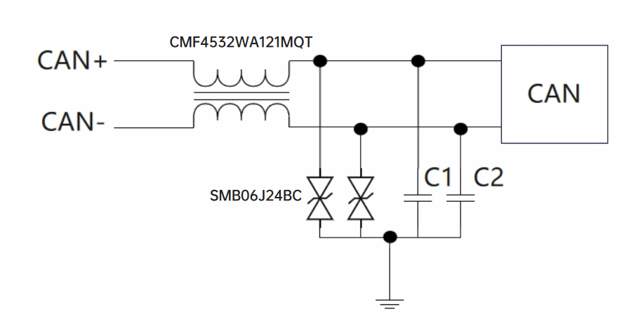
2026.07.20
How should a failure in the CAN communication surge test be handled?
2026.07.22
Why Should ESD Protection Devices Be Placed Close to Interfaces? An Analysis of PCB Layout and Discharge Paths
2026.07.23
How do you implement ESD protection for USB Type-C interfaces? You need to select separate solutions for the data lines, CC lines, and VBUS.
2026.07.23
How to Design ESD Protection for HDMI Interfaces? Key Selection Criteria for TMDS High-Speed Lines and Control Lines
2026.07.24
What are the differences between SMA, SMB, and SMC packaged TVS diodes? Selection based on power and size.
2026.07.24
How to Select a TVS Diode for the Power Input: A Complete Process from Operating Voltage to Clamping Voltage
2026.07.25
What are the differences between load dump, surge, and ESD? Strategies for automotive power supply transient protection.


