Submit






An ESD protection diode manufacturer should be evaluated through six observable capabilities: product definition, parameter testing, package control, application validation, lot traceability, and failure analysis. Company size and part count provide background. Engineering evidence determines whether a supplier can support qualification and stable production.
Capability one begins with a datasheet that can be audited
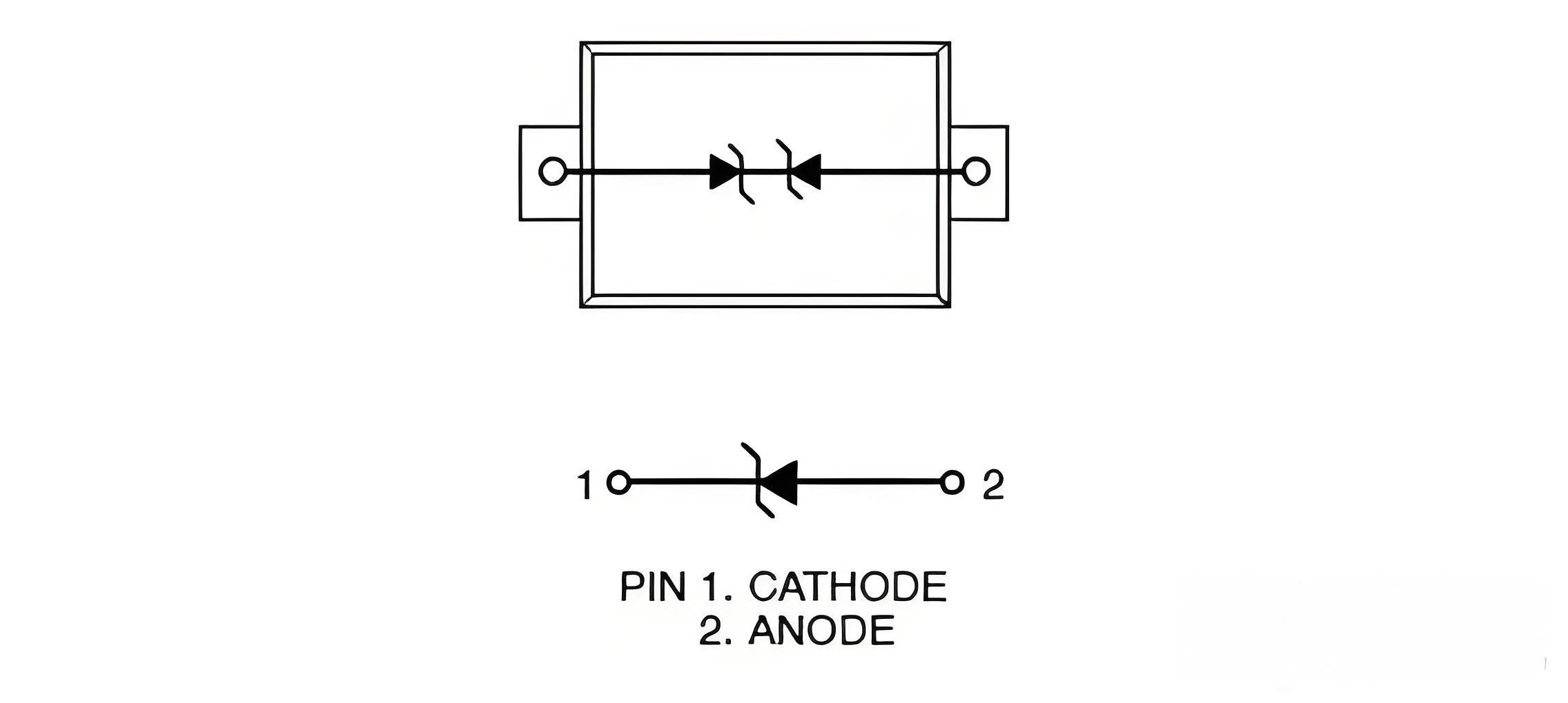
A datasheet is an early view of the manufacturer's engineering discipline. Clamping voltage needs a stated pulse current or waveform. Junction capacitance needs a frequency and bias condition. Leakage current needs the applied voltage and temperature. Polarity, internal topology, package drawing, pin assignment, and ordering code must agree throughout the document.
Ask for the following items during the first review:
minimum, typical, and maximum labels for electrical values;
current, waveform, frequency, and temperature conditions;
package dimensions, orientation mark, and recommended land pattern;
operating and storage temperature information;
packaging method, document revision, and change history.
A short datasheet can be adequate when these definitions are present. A long document is still difficult to use if the conditions are missing or if related products use inconsistent definitions.
Capability two is low-capacitance design with a stated boundary
High-speed interfaces need low loading, but a small typical capacitance number does not complete the design. Package parasitics, routing branch length, channel matching, and reference-plane transitions all affect signal quality. The manufacturer should explain how capacitance was measured and which interface conditions the candidate is intended to address.
Build an evaluation board or reserve assembly options for an unpopulated state and two candidate devices. Compare eye behavior, link training, error rate, hot-plug operation, and the target ESD test. One candidate can prioritize signal margin while another retains more clamping margin. This comparison exposes the real tradeoff instead of turning capacitance into a single-variable contest.
The protected IC remains part of the decision. An ultra-low-capacitance device may have a different dynamic resistance or clamping response than a higher-capacitance option. If the IC has a narrow transient tolerance, the signal and protection margins must be reviewed together.
Capability three is dynamic clamping that can be interpreted
An ESD withstand rating answers whether the component survived a defined stress. Clamping data answers how the voltage behaves while current flows. The system needs both, because a protector can survive while allowing a damaging voltage at the IC pin.
Use a controlled sequence for clamping review:
Define the normal electrical window and the protected node's absolute maximum rating.
Compare devices at the same pulse current or waveform.
Measure the transient at the protector and, where practical, at the protected node.
Inspect leakage, standby current, and function after repeated stress.
Modify placement or return geometry and repeat the same measurement.
Test a second lot before the device is approved for production.
Board inductance adds voltage during a fast current change. A short value in a datasheet cannot include every connector, pad, via, and return layout. The manufacturer should separate known device data from the items that remain a system measurement.
Capability four is package control that survives assembly
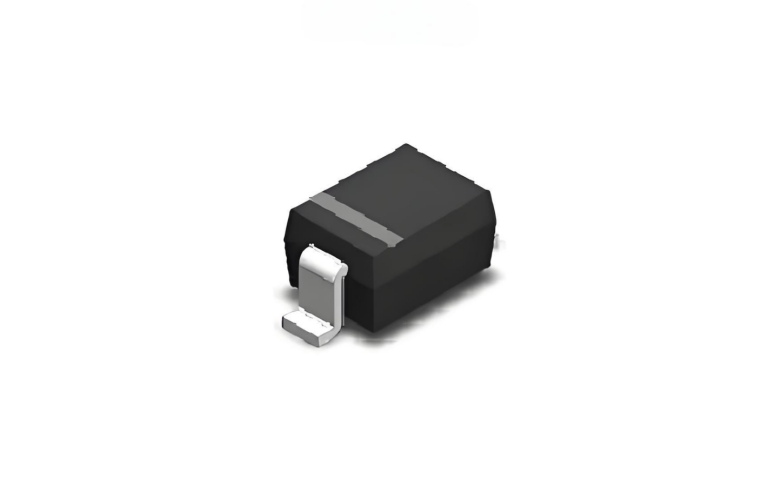
Small ESD packages save board area, but they demand accurate land patterns, orientation control, coplanarity, stencil design, and inspection. A device that performs well in a lab can still create production loss if markings are difficult to recognize or if the recommended pad geometry is unclear.
Review the complete current path through the package. The entry trace, protector pad, return pad, and vias form part of the transient circuit. A long lead, a side branch, or an asymmetric array footprint can raise dynamic voltage or disturb a differential channel. The package review therefore covers electrical parasitics and manufacturing yield at the same time.
Production teams should record reflow conditions, automated optical inspection rules, polarity checks, and rework limits. These records become especially useful when an intermittent failure appears only after assembly or after a footprint revision.
Capability five is lot control and change communication
The first sample lot proves that a candidate can work. It does not prove that later deliveries will reproduce the result. Qualification needs lot identification, packaging consistency, incoming inspection criteria, and a formal path for material, process, site, or package changes.
Select the tests most sensitive to variation and repeat them on another lot. For a high-speed device, that set may include capacitance-related signal checks and leakage. For a power-facing protector, it may include clamping, pulse response, and thermal behavior. Keep the board, fixture, operating state, and acceptance criterion fixed.
Traceability should continue into a returned failure. The supplier needs the shipped lot, device marking, application condition, stress history, and failure symptom. Without this chain, a laboratory can report that a loose sample is electrically normal while the production issue remains unresolved.
Capability six is failure analysis that tests competing explanations
Useful failure analysis starts by reproducing the symptom and separating four possible causes: device damage, assembly defect, PCB discharge path, and insufficient tolerance at the protected circuit. The plan may include electrical retest, visual inspection, package analysis, comparison with an unused device, and a controlled board experiment.
An answer such as “sample passed retest” is incomplete when the system failure remains repeatable. The manufacturer and customer should align the device result with the board revision, discharge point, polarity, cable state, software mode, and recovery behavior. A conclusion should state what was observed, what was ruled out, and what must be tested next.
Applying the six checks to ASIM
ASIM can support ESD device selection together with EMC test and remediation review. That combined workflow helps a customer compare the electrical window, layout path, and observed system response without treating each as an unrelated task. It also creates a direct route from sample selection to a controlled board experiment when the first test fails.
ASIM devices should pass the same six checks used for every production candidate. Brand identity shortens communication; it does not replace evidence. The final approval record should state the part number, document revision, lot, board, test method, operating condition, and remaining application limits.
The strongest supplier relationship is one in which both parties can explain why the device was selected and when the decision must be reviewed again. That standard supports purchasing continuity, engineering confidence, and a cleaner response when a later product revision changes the electrical boundary.
Questions about manufacturer capability reviews
Does a large ESD product catalogue prove strong design capability?
No. Audit related datasheets, test definitions, sample support, and lot control, then validate a candidate on the intended interface.
Can an ESD diode without public TLP data still be considered?
Yes, but dynamic clamping remains an open item. Add board-level transient and post-stress measurements before approval.
Why should a manufacturer review the PCB layout?
The protection current flows through pads, traces, vias, and a return reference. A correct device on a poor discharge path can leave excessive voltage at the protected circuit.
 Previous