





 Submit


ESD5E001TA Low-Capacitance ESD Diode for 5 V Signals
 2026.08.19 00:00:00
 40
40





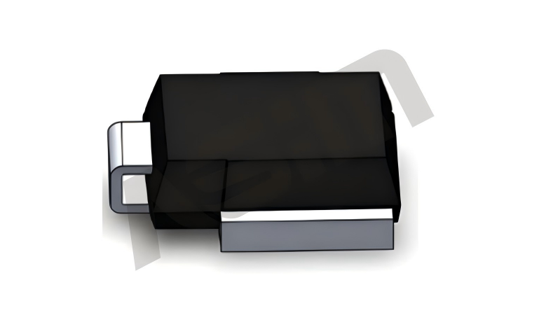
ESD5E001TA uses a bidirectional DFN0603-2L package. It has a 5 V reverse working voltage, 6 V minimum breakdown, 2.5 A peak pulse current, 18 V maximum clamp at the stated condition, and 0.08 pF typical junction capacitance. The low capacitance makes it a candidate where signal loading matters, but the finished channel remains the decision point.
Begin with the circuit condition
A 0.08 pF typical value is measured under specified conditions. It is not a guarantee that every connector, trace, receiver and cable assembly will show the same signal result. Start with the maximum normal voltage, the actual signal swing, the receiver’s absolute maximum rating and the test requirement. Then review the transient current path from the connector through the diode to the intended return copper.
The device data must be read with its stated test conditions. A clamping number is tied to a pulse current and waveform. Capacitance is tied to bias and frequency. Neither value includes the trace inductance between a connector, a protection component and a protected pin. Put those three locations on one layout print before deciding whether a part is suitable.
List the normal states that can occur on the exposed net. Include the highest steady voltage, polarity, power-up sequence, cable state, load and any external equipment that can drive the line. This avoids selecting a part from the nominal voltage label while missing a valid operating condition. The receiver’s absolute maximum rating and internal clamp structure also belong in the same review.
Use the part number with a defined selection sequence
Start from normal operation, then move toward the disturbance condition. The reverse working voltage should cover the measured operating window. Breakdown tells where conduction begins under the defined condition. The clamp value must be compared at the specified current and waveform, then checked against the downstream voltage limit. Package, leakage and capacitance complete the electrical review.
Identify the external energy entry point and the protected node.
Record the maximum normal voltage and all power-sequence states.
Read working voltage, breakdown and clamp values with their conditions.
Check capacitance, leakage, footprint and the protected-circuit limit.
Verify the selected device on the production-intent PCB.
Keep a short evidence list with the schematic net name, connector pin, measured normal voltage, board revision and protection footprint. These details make later changes traceable. They also prevent a valid result on one cable or one board revision from being applied to a different configuration without review.
Make the protection path physically short
Place the protection component close to the external entry, before a long internal trace. Its connection to the intended high-frequency return should be short, wide and continuous. A narrow neck, an indirect via path or a route around a split reference plane can add inductance and raise the voltage seen by the protected circuit during a fast event.
For a small package, inspect the pad escape and nearby return via rather than judging only by the component’s distance from the connector. For a high-speed signal, check the stub created by the connection and preserve the symmetry of paired routes. For an input TVS, draw the route from connector through the TVS return and into the power stage. The drawing should make clear where transient current flows.
Keep the connector-to-protection segment short.
Avoid routing the protected net through a long branch before the device.
Keep sensitive reset, clock and analog nodes away from the return path.
Treat temporary copper or wire changes as diagnostics, then review the production layout separately.
Test the board instead of the datasheet alone
Use an unchanged sample as the baseline. Change one variable at a time: device selection, placement, return connection or a single layout feature. Repeat the target stress with the same supply, cable, load, firmware and measurement method. Restore the baseline for an A/B/A comparison when the result matters. This step catches apparent improvements caused by a different operating mode or test setup.
Observe more than catastrophic failure. Record reset activity, standby current, communication errors, link recovery, data integrity, temperature and recovery time. A product that remains powered may still have an unacceptable functional interruption. If a temporary shielding or routing change identifies a path, document the path; do not convert one temporary observation into a general claim about all applications.
Keep the review tied to the released design
The selected component belongs to a particular schematic, footprint, PCB revision and test configuration. A cable change, enclosure change, supplier substitution or firmware power-sequence change can alter the conditions that were originally checked. Review the selection again when one of those boundaries moves. The recheck does not always require a full test campaign, but it should address the change that affects voltage, current path, capacitance, leakage or functional behavior.
For a useful release record, include the component marking, placement image, return-via arrangement, sample count, cable condition and the observed functional result. A later engineer should be able to repeat the test without guessing which bench setup produced the original result. This is especially important for interface and input protection, where layout changes that appear small can move the transient path by a large electrical distance.
Release evidence and common questions
Can a similar package be substituted directly?
No. Confirm the normal voltage window, polarity, clamp condition, capacitance, pad geometry, return path and the measured behavior of the assembled board.
Does the lowest clamp value always provide the safest result?
No. Read it with its pulse current and waveform. A part also has to fit normal operation, leakage, capacitance, package limits and the physical current return.
When can the choice be released?
Release it after normal function and the target stress have been repeated with the documented board, component placement and test configuration. Keep that record with the released board revision.
 Previous

Related News

2024.10.12
EMC testing Contents and Current Situation of Automotive Electronic products
2026.07.16
How do you design a surge protection solution for industrial power supplies?

2026.07.28
Why does adding a filter fail to resolve EMC issues? First, determine whether the noise is common-mode or differential-mode.

2026.08.06
Why TVS Diodes With the Same VRWM Have Different Clamping Voltages
2026.08.07
How to Estimate TVS Diode Dynamic Resistance From VC and IPP
2026.08.08
Why Does TVS Diode VBR Change With Temperature?


