Submit






A low-capacitance ESD diode should not be selected by sorting junction-capacitance values from smallest to largest. Capacitance must be read with measurement frequency, DC bias, temperature, and typical or maximum definition. The same review must cover line voltage, signal rate, channel matching, leakage, clamp behavior, package, and PCB branch geometry. A very small device capacitance cannot repair a long T-branch or an asymmetric footprint.
Make capacitance values comparable before ranking parts
One supplier may publish 0.2 pF at zero bias, another 0.25 pF without a stated frequency, and a third 0.5 pF as a maximum over voltage. Those numbers are not ready for direct ranking. The voltage dependence of the junction can change the channel load during operation, while a typical figure does not define the production limit.
Build a candidate table with these fields:
capacitance test frequency, DC bias, temperature, and statistical definition;
reverse working voltage and the highest and lowest valid line voltage;
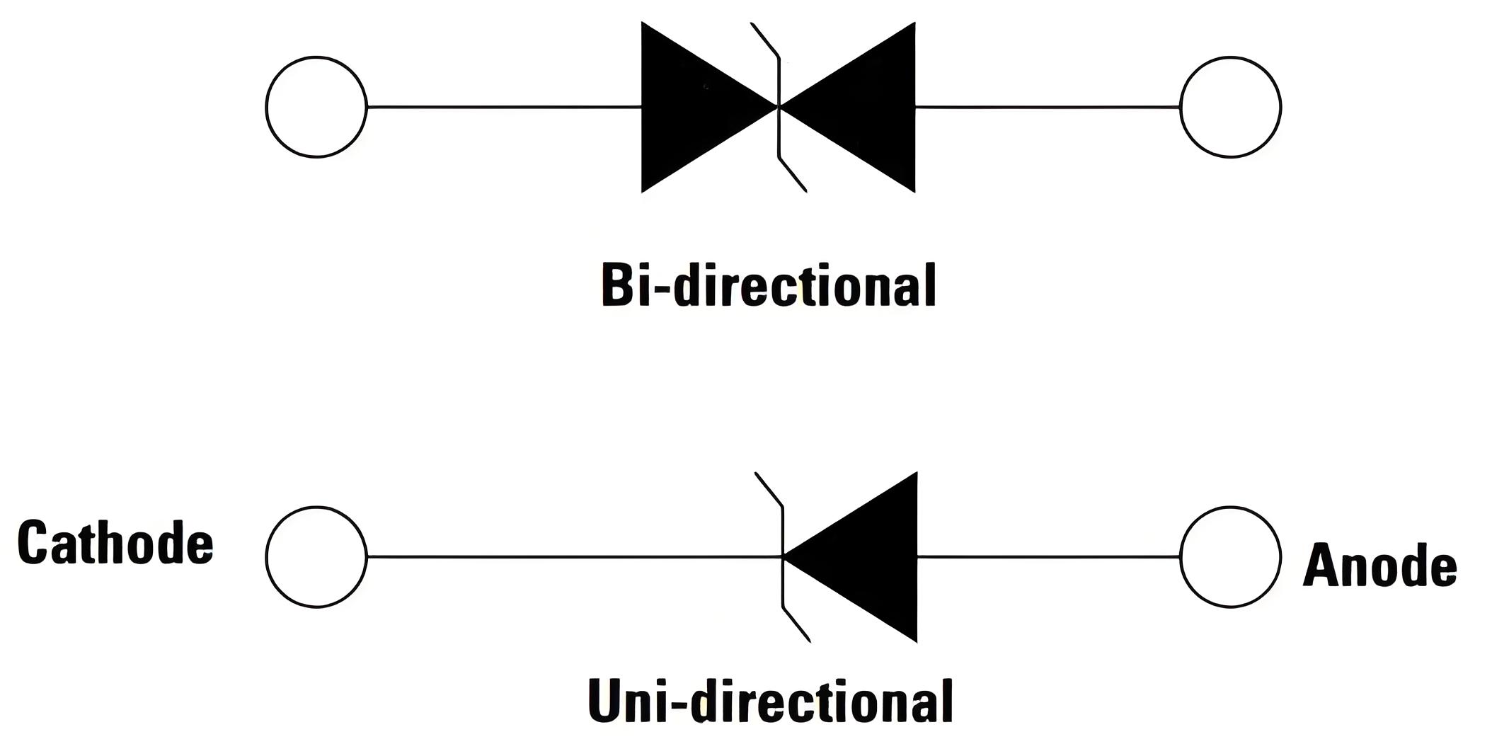
unidirectional or bidirectional topology and channel structure;
reverse leakage with its voltage and temperature condition;
package, land pattern, pinout, and channel matching information;
clamp voltage with pulse current and waveform;
target insertion loss, return loss, eye margin, or error rate.
If a data sheet does not provide a needed condition, ask the manufacturer before treating the number as equivalent to another device. A missing maximum capacitance can matter more than a slightly lower typical value.
Treat pads, vias, and branches as part of the channel
The assembled channel contains more than the silicon junction. Package leads or lands, pads, escape routing, vias, connector transitions, and stubs add capacitance and inductance. A protection device placed 20 mm away on a side branch can create a resonant discontinuity and still allow the fast transient to reach the receiver first.
The preferred current path is external connector, protection pad, and then internal signal route. Connect the device return to a continuous reference plane through short, nearby vias. Avoid a narrow ground neck shared with a reset, oscillator, or analog reference circuit.
Use a controlled board evaluation:
Save the channel baseline with the original or unpopulated protection position.
Change only the ESD diode while keeping the PCB, cable, fixture, and software constant.
Measure the target data mode, eye diagram, insertion loss, or error rate.
Repeat the functional test during normal, standby, hot-plug, and powered-off states.
Apply the required system-level ESD configuration.
Recheck signal performance, leakage, and device condition after stress.
Restore the original configuration and repeat the candidate to confirm the direction.
A result collected from two different board layouts cannot isolate the device capacitance.
Separate signal loading from clamp performance
Junction capacitance describes part of the small-signal loading. Clamp voltage describes device-terminal behavior at a stated pulse current and waveform. Lower capacitance does not guarantee lower VC, lower dynamic resistance, or greater pulse capability. High-speed protection needs all three boundaries: valid normal operation, acceptable signal integrity, and residual voltage below the receiver limit.
An ASIM low-capacitance ESD family can be screened by 3.3 V or 5 V working class, number of channels, topology, and package. Exact models may be used inside engineering evidence, but the useful content target is the selection method rather than an isolated part-number page. The reader needs to understand which conditions make a parameter meaningful.
Measure at both the protection device and the receiver when practical. The voltage difference shows the overshoot created by the package and PCB path. A favorable catalog clamp number can be defeated by several nanohenries in the return route.
Review shared paths in multi-channel arrays
Multi-channel arrays reduce placement area and part count, but channels can share a reference terminal or internal structure. Do not group lines with different voltage domains, polarity requirements, powered-off behavior, or failure consequences just because spare channels are available.
Differential pairs also need channel and routing symmetry. Unequal pad geometry, branch length, or channel loading can convert differential energy into common-mode current. The design may then lose eye margin and create a new EMI problem at the same time.
Map every array channel to one connector pin and one receiver pin. Record unused-channel treatment, orientation, and return-via placement in the layout review. This channel map should remain tied to the approved BOM and board revision.
Questions from high-speed protection reviews
Is 0.1 pF always better than 0.5 pF?
No. Compare values under the same measurement conditions and include leakage, clamp performance, package parasitics, PCB geometry, and the target-rate board result. A lower catalog number can produce a worse assembled channel.
Do slow control lines require the lowest available capacitance?
Many slow lines have a wider capacitance budget. Working voltage, leakage, threshold, polarity, power sequencing, and transient return path often deserve higher priority than the minimum Cj value.
Can unused array channels protect a different interface?
Only when voltage, polarity, capacitance, shared return, channel topology, and fault isolation are compatible. An unused pin is not evidence that unrelated lines should be combined.
The final approval should state interface mode, line voltage, data rate, capacitance condition, board revision, device location, signal result, and post-ESD function. Avoid a conclusion such as lower capacitance is always better; record the boundary that the assembled product actually passed.
Production release should also preserve the exact package orientation, channel assignment, and approved land pattern. Repeat the most sensitive signal test on representative boards from normal assembly, because solder volume and placement offset can change a sub-picofarad discontinuity. If an alternate supplier is introduced later, compare it against the stored channel baseline rather than against a verbal claim of equivalent capacitance.
 Previous