Submit






A low capacitance value does not qualify an ESD protection diode for USB4 or HDMI 2.1. At multi-gigahertz frequencies, package inductance, mounting pads, protection branches, return paths, and resonance affect insertion loss and reflection. S-parameters and target-link tests are needed alongside capacitance and clamping data.
Equal capacitance does not create equal RF behavior
Junction capacitance is measured at a stated frequency, reverse bias, and signal level. The mounted channel also contains package inductance, pad capacitance, vias, stubs, connector discontinuities, and the return connection. Two devices listing 0.25 pF can reach different resonances and add different attenuation or reflection after mounting.
Ask the manufacturer for the capacitance condition, whether the number is typical or maximum, S21 insertion-loss and S11 return-loss curves, the test board, reference plane, port impedance, and de-embedding method. Package and recommended-land information are part of the RF data, not a drawing to inspect after the device has been selected.
A practical manufacturer data request includes:
capacitance frequency, bias, sample definition, and channel matching;
S21 and S11 magnitude across the relevant frequency span;
single-ended or differential fixture impedance and port mapping;
package, land pattern, and ground-return recommendation;
working voltage, leakage, clamping, dynamic resistance, and ESD conditions.
Missing S-parameters do not prove the part is unusable. They transfer more measurement work and uncertainty to the customer.
Divide the connector into electrical line groups
USB Type-C contains high-speed differential pairs, USB 2.0 D+ and D-, configuration-channel pins, sideband-use pins, and VBUS. They do not share one voltage or bandwidth model. HDMI also combines high-speed lanes with lower-speed control and utility lines. A single “low-capacitance ESD for the connector” recommendation can be electrically wrong for part of the pin set.
| Line group | Manufacturer data to screen | Target-board result to verify |
|---|---|---|
| USB4 high-speed pairs | S21, S11, package parasitics, and matching | Link training, errors, eye or channel metric |
| USB 2.0 and control pins | Voltage window, leakage, capacitance, and clamping | Enumeration, control function, and post-stress state |
| HDMI high-speed lanes | Insertion loss, reflection, balance, and layout | Intended video/link mode and signal test |
| HDMI lower-speed pins | Actual voltage, polarity, and interface state | Hot plug, control function, and ESD result |
The part selection should be recorded per line group. Copying the voltage on VBUS into a high-speed data-line choice is a common way to obtain excessive clamping voltage or capacitance.
Use S21 and S11 as screening curves
S21 describes forward transmission from input to output; its insertion-loss presentation shows attenuation added by the device and fixture. S11 describes the reflected portion at the input and helps expose impedance discontinuity. Both need a frequency range related to the intended channel and a common fixture before devices can be compared.
Apply the curves in a controlled order:
Confirm the manufacturer’s test board, reference plane, impedance, and de-embedding.
Mark the frequency range relevant to the intended protocol mode and board budget.
Compare S21 attenuation, S11 reflection, and resonant behavior.
Import the land pattern and model into a channel review when available.
Measure the final branch with connector, vias, protection device, and PCB reference.
Repeat the link test after ESD stress to detect damage or parameter drift.
A curve that extends to a high frequency is not automatically good data. The reference board and measurement definition decide whether the curve represents the customer’s mounting condition.
Do not trade away the protection window for capacitance
High-speed compatibility is one gate. Reverse working voltage must cover every normal line state without unwanted conduction. Leakage must fit the bias network. Clamping voltage and dynamic resistance must keep the protected IC within an acceptable transient boundary after package and PCB overshoot are included.
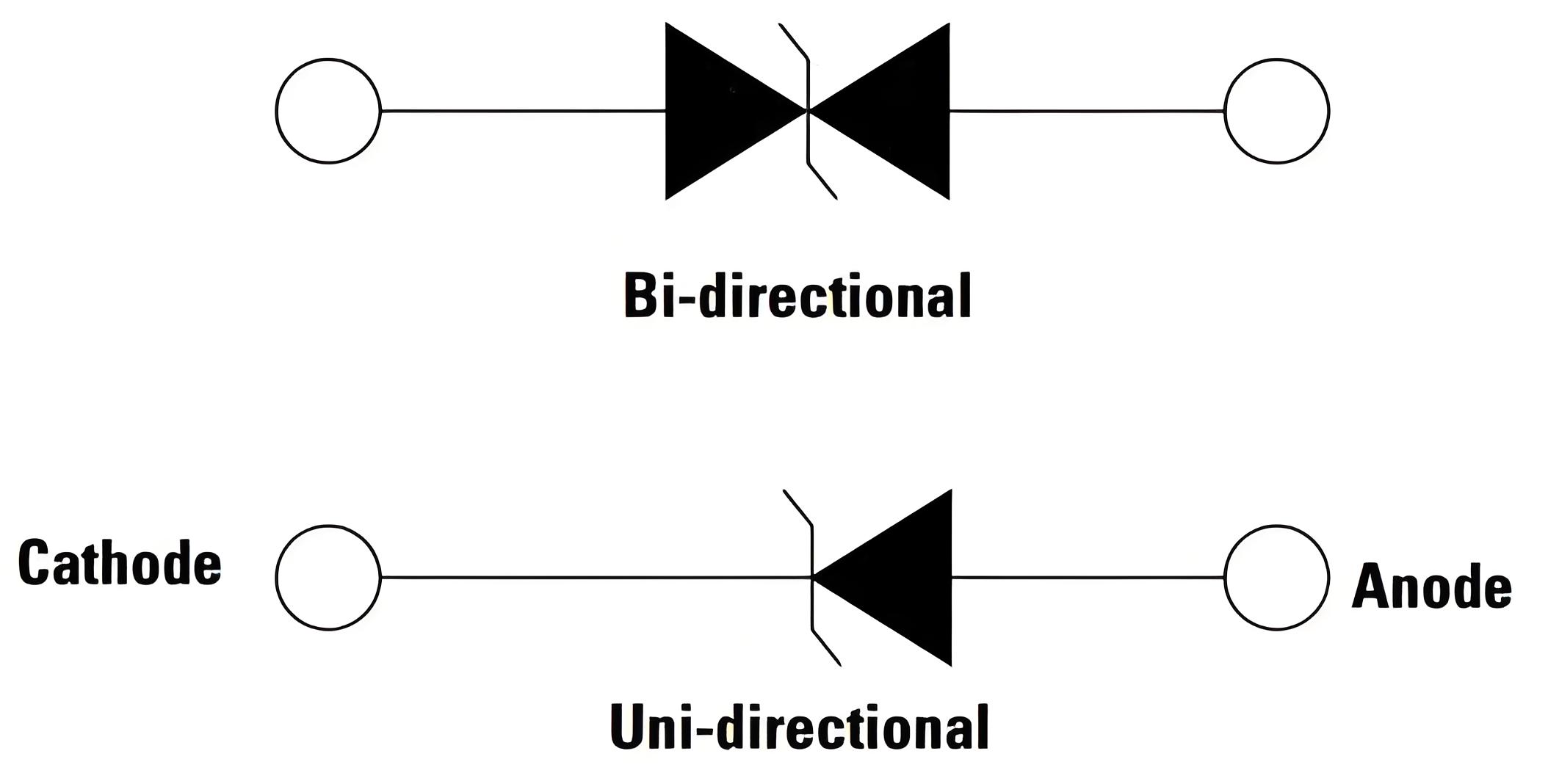
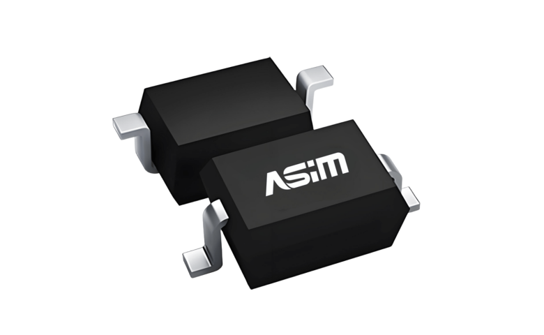
ASIM ESD3V3X004SA and ESD5X004SA are bidirectional four-channel arrays in DFN2010-5L, both listing 0.25 pF typical junction capacitance. Their reverse working voltages are 3.3 V and 5 V, and their minimum breakdown voltages are 4.2 V and 6 V. The shared capacitance and package do not make the voltage options interchangeable.
For a USB4 or HDMI 2.1 design, these published values can place a device in the candidate set. They do not replace S-parameter conditions, channel simulation, target-mode operation, layout review, or system ESD validation.
Evaluate the manufacturer through reproducible data
A useful low-capacitance ESD manufacturer can connect the full order code to parameter conditions, RF curves, sample lots, mounting guidance, and an application response. The customer should preserve the device-data revision, PCB files, channel result, ESD setup, and post-stress state in one release record.
The ASIM ESD diode manufacturer hub provides the broader manufacturer, product, and application path. This high-speed page answers a focused question: why capacitance alone does not qualify USB4 or HDMI 2.1 protection.
When a connector, package, PCB stack-up, or protocol mode changes, the record shows which RF and ESD checks must be repeated. That is more useful than reopening a generic debate about whether 0.25 pF is “low enough.”
Retain the unprotected channel baseline as well; without it, the ESD device may receive blame for loss already created elsewhere in the layout.
Questions about low-capacitance ESD manufacturers
Does the lowest capacitance guarantee the best high-speed performance?
No. Package inductance, pads, resonance, branch layout, matching, insertion loss, and reflection also affect the channel.
Can one ESD array protect both USB4 and HDMI 2.1?
Only if voltage, topology, channels, RF behavior, layout, clamping, and target-link tests fit both applications. The interface names do not establish compatibility.
What if the manufacturer does not provide S-parameters?
Measure candidates on a controlled fixture and the target board. Production approval still needs a reproducible channel result and system ESD result.
Copyright notice:Copyright belongs to Shenzhen ASIM Electronics Co., Ltd. Please retain the author, source, and original URL when quoting or republishing.
Original URL: https://asim.com.cn/low-capacitance-esd-manufacturer-usb4-hdmi21-en.html
 Previous