Submit






When system ESD testing still fails after the protection diode is replaced, do not immediately try another device with a higher catalog level. Verify that the transient reaches the protection node before the IC, that the device has a short return to its high-frequency reference, and that the observed failure actually enters through the signal line. Correct component parameters solve only one part of the protection network.
Three device changes produced the same MCU reset
On one board, three candidate ESD devices had different catalog ratings, yet the failure threshold barely changed. Measurements at the protection device and MCU pin showed that the device was clamping, while the receiver still saw a large overshoot. The connector trace continued toward the MCU and the suppressor sat on a long side branch. The fast transient reached the receiver before enough current turned into the branch.
Capture the original failure with:
- discharge point, polarity, contact or air method, and operating state;
- failure type such as reset, freeze, disconnect, data corruption, or damage;
- physical locations of connector, protection device, IC, and reference plane;
- waveforms at the device, receiver pin, power rail, and reset pin;
- reset reason, communication error, or retained event log;
- the single variable changed for each A/B test.
Without this baseline, replacing parts produces a stack of anecdotes rather than a diagnosis.
Inspect the route from connector to protection pad
The external signal should pass through the protection landing area before it continues into internal circuitry. A long T-branch adds inductance and allows current to continue along the main route. Moving to a larger package at the same bad location can increase channel loading without reducing receiver overshoot.
Use a controlled diagnostic sequence:
- Reproduce the failure in the original configuration and read the event log.
- Compare voltage at the protection terminal and receiver pin.
- Shorten the connector-to-device path with a temporary, controlled modification.
- Shorten the device return and add nearby reference vias.
- Test signal, power, reset, enclosure, and cable paths as separate variables.
- Restore the original condition and repeat the effective change.
- Transfer the temporary fix into a manufacturable PCB and enclosure design.
A temporary wire or copper strip proves a physical direction. It does not become the production design without creepage, signal integrity, assembly, and reliability review.
Inspect the return from the suppressor to its reference
A ground symbol on the schematic does not guarantee a low-impedance transient return. A narrow neck, distant via, plane slot, or shared analog island develops voltage during the fast current pulse. Multi-channel arrays can raise the reference of several lines at once when their common terminal uses the same inductive path.
Place return vias next to the protection pad and connect to a continuous plane appropriate for the interface. If a connector shell or cable shield should carry the discharge, provide a controlled chassis path rather than force the current through digital ground. Measure whether the modification changes the device-to-IC voltage difference.
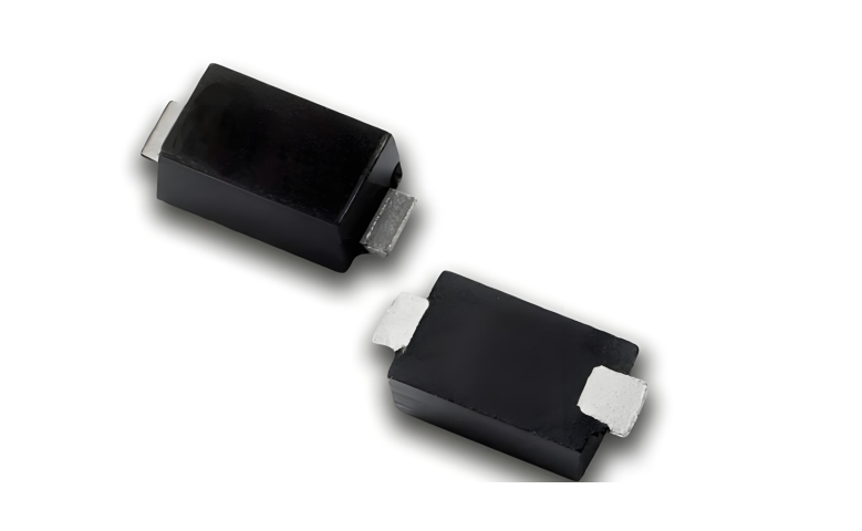
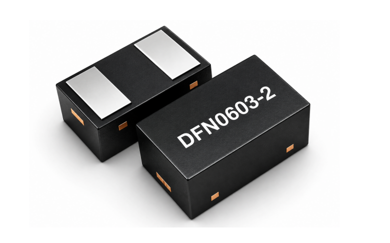
ASIM ESD diodes should be screened by working voltage, clamp condition, capacitance, leakage, topology, and package. Layout acceptance remains a separate requirement. Exact model numbers can appear in a qualification record, but they no longer need to be the website's primary search topic. The useful answer explains when the parameter works and when the path defeats it.
Change direction when the signal pin is not the first victim
Discharge can couple through a metal enclosure, cable shield, power input, reset trace, oscillator, or board-to-board cable. Read the MCU reset source when available. Brownout points toward power or ground shift; external reset points toward RESET coupling; watchdog reset may follow a communication lock or software exception.
If the protection-device waveform improves while the failure remains unchanged, inspect common power, reference, and high-impedance nodes. Monitor the rail at the affected IC rather than only at the regulator output. A local decoupling path or narrow power neck can hide the disturbance from a remote probe.
Software retry can improve user recovery, but it does not prove hardware stress is controlled. Record hardware voltage, functional interruption, recovery time, stored data, and safe output as separate results. The product performance criterion determines whether automatic recovery is acceptable.
Re-select the device only after the path is credible
Return to component selection when the connector route and reference path are short, yet device-terminal clamp voltage, leakage, capacitance, or pulse capability still fails the design boundary. Use the measured line voltage, actual pulse current, receiver tolerance, and comparable waveform conditions. Avoid trial selection by higher ESD level alone.
Repeat the final configuration with fixed sample, cable, software, discharge point, interval, polarity, and worst operating state. Pre-compliance improvement demonstrates direction; formal compliance still requires the applicable standard setup and agreed product criteria.
Questions after a protection-device swap
Why does a higher component ESD level fail to improve the system?
Component ratings do not include the enclosure, connector branch, PCB return, cable path, receiver state, or system performance criterion. A transient that bypasses the device will not be fixed by the printed level.
Does normal voltage at the TVS terminals prove that the IC is protected?
No. The IC pin can see added overshoot from trace and return inductance. Measure at the receiver and compare with its permitted boundary.
Is automatic software recovery enough to close the failure?
Only when the product criterion explicitly allows that behavior and hardware stress, recovery time, data integrity, and safe output have all been verified.
The closing report should identify the verified current path, the effective single-variable change, device conditions, board revision, receiver result, and formal retest configuration. That evidence prevents the next failure from starting with another blind component swap.
 Previous