Submit






AI glasses place exposed interfaces close to sensitive processors, cameras, displays, radios, and compact power circuits. ESD protection therefore cannot be handled by adding one low-capacitance diode to every net. Charging contacts, USB-C pins, camera lanes, keys, and frame metal each need a protection path matched to normal voltage, bandwidth, user contact, and return structure.
A small enclosure does not create a small ESD problem
AI glasses combine wearable contact, frequent charging, high-speed data, cameras, audio, radios, sensors, and a battery inside a constrained frame. The product is handled near the face, placed on different surfaces, carried in pockets or cases, and connected to chargers or accessories. Those uses create several discharge entry points even when the exterior appears mostly plastic.
The engineering task is to keep transient current away from sensitive silicon while preserving signal quality. That requires an interface map before choosing a protection device. Mark every exposed conductor, nearby seam, button, charging contact, connector shell, flex transition, and metal decoration. Then identify where current can return to the source. A protected signal without a low-inductance return can still develop a damaging residual voltage.
Treat the charging contacts as a power-entry problem
Pogo pins or magnetic charging contacts can be touched directly and may carry power, ground, identification, or communication. The power pin can also experience hot-plug overshoot, charger-cable transients, and ESD. These events do not share the same waveform, so a single pass or fail label is not enough.
Start with a measurement of the actual power window. Record charger tolerance, battery-management states, cable and contact resistance, no-load behavior, and the highest repetitive overshoot during attachment and detachment. The protector's reverse working voltage must remain above this normal boundary. Its clamping behavior must then be checked against the downstream power-management pin, including voltage added by package and layout inductance.
A charging-contact review follows this order:
Measure the highest normal and hot-plug voltage at the board entry.
Identify which contacts a user or charged object can reach first.
Place the protector near the contact entry, ahead of the sensitive branch.
Give transient current a short, wide return to the intended ground structure.
Test contact sequences, charger orientations, operating states, and both ESD polarities.
Recheck leakage and charging behavior after the immunity sequence.
Do not route the transient return through a narrow battery-ground trace that passes under the processor. That layout can convert a protected contact into a board-wide disturbance.
USB-C needs pin-by-pin electrical boundaries
USB-C can include VBUS, CC, USB 2.0 data, high-speed differential lanes, shield, and optional mode functions. Applying one device type to all pins usually creates an electrical risk or unnecessary signal loading.
The D+ and D− lines and any SuperSpeed lanes need protection with capacitance and S-parameter performance appropriate to the implemented data rate. CC pins need a normal-voltage window that includes attachment and role behavior. VBUS needs a power transient solution selected for its highest legitimate voltage, including power-delivery operation if present. The shell needs a deliberate connection to the chassis or reference structure rather than an accidental path through signal ground.
For every protected USB-C pin, verify:
maximum continuous voltage and legitimate overshoot;
direction and number of protected channels;
leakage at operating temperature;
capacitance and insertion or return loss over the required band;
clamping voltage at a relevant transient current;
pin mapping, connector orientation, and flow-through layout;
distance from the receptacle to the protector and return vias.
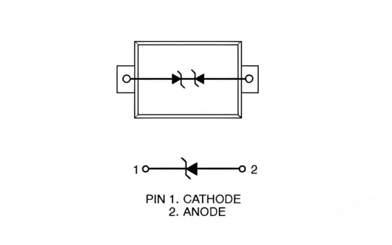
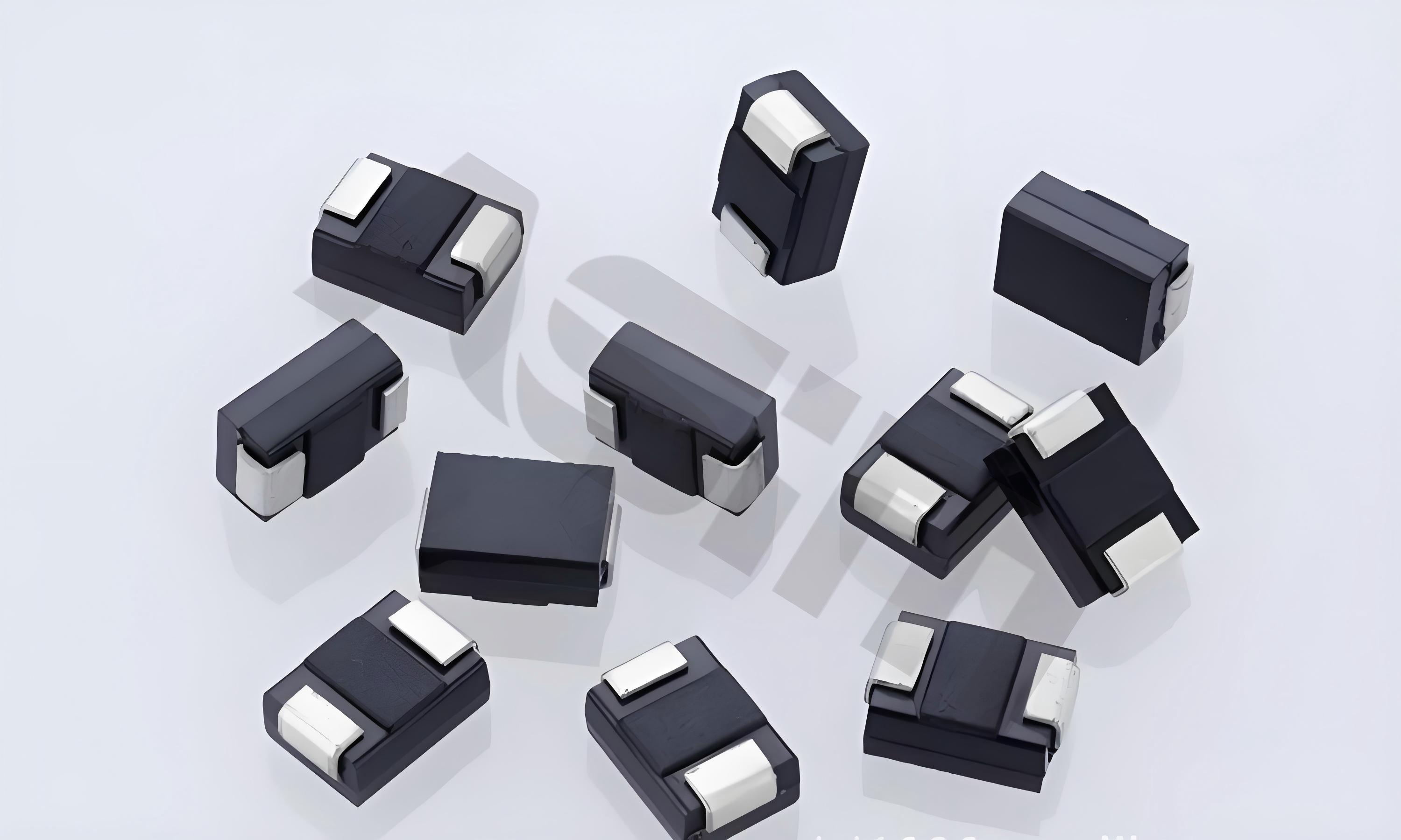
ASIM ESD3V3X004SA and ESD5X004SA illustrate why voltage class remains part of the discussion even when two arrays share a bidirectional four-channel DFN2010-5L format and a published typical junction capacitance of 0.25 pF. Their reverse working voltages are 3.3 V and 5 V respectively. The correct candidate depends on the real pin voltage and the complete channel, not on capacitance alone.
Camera and display lanes are signal-integrity decisions
MIPI camera and display links can be sensitive to added capacitance, discontinuity, channel mismatch, stub length, and poor pad geometry. A protection part that survives a component pulse can still reduce eye margin when its package and footprint are inserted into the assembled lane.
Use a flow-through layout where the package supports it. Keep the branch to the device short, preserve differential symmetry, and avoid unnecessary layer changes. Request the Touchstone file, port definition, reference impedance, fixture information, and de-embedding boundary. Compare those data with the frequency content of the implemented link rather than relying on a generic high-speed label.
Validation should include the complete path: image sensor or display, flex cable, connector, protection package, PCB traces, processor, clock plan, and intended operating modes. Capture link errors, image artifacts, startup reliability, and margin before and after ESD testing. A clean eye diagram on a separate coupon does not prove that the folded flex and production enclosure behave the same way.
Keys, microphones, and sensors can carry current deeper into the frame
A metal key cap, microphone opening, speaker mesh, touch electrode, hinge, or decorative strip may couple a discharge into a nearby flex cable without being electrically connected to the signal. Protection at the processor end can be too late if current travels along the flex and crosses several subsystems first.
Inspect the physical stack-up as well as the schematic. Shielding films, conductive coatings, frame fasteners, adhesive gaps, and flex-ground fingers can redirect current. A local protector may be needed at the exposed end, while a controlled chassis bond carries most of the event away from logic ground. For capacitive touch and analog sensor lines, leakage and capacitance must be checked against sensing thresholds and calibration behavior.
Test realistic operating states, not one convenient screen
Wearable products change susceptibility with radios, cameras, displays, charging circuits, audio paths, and processors active. A unit that passes while idle can reset or corrupt data when a high-current task changes the power impedance or when a camera flex is switching.
Build a compact state matrix rather than testing every theoretical combination. Include charging and battery operation, camera streaming, display activity, wireless transmission, audio, low-battery conditions, wake and sleep transitions, and accessory connection where applicable. Choose representative worst-case states through pre-scan measurements and risk analysis, then keep them fixed during the formal comparison.
Monitor more than visible resets. Record link recovery, frame errors, battery-management faults, current consumption, audio artifacts, storage integrity, and software logs. A product that silently disables a camera until the next reboot has not simply recovered.
Protection closes with current-path verification
An AI-glasses ESD design is ready for validation when each entry point has a named protected circuit, a defined normal operating window, a short current path, and a measurable acceptance criterion. Device specifications are necessary, but placement and return geometry often decide the first nanoseconds of the event.
ASIM supports ESD and TVS selection from interface conditions outward. The ASIM ESD diode manufacturer hub provides a stable route to related selection material. Final approval should use the exact product data, production footprint, assembled frame, cables, firmware, and operating modes intended for shipment.
Copyright notice:Copyright belongs to Shenzhen ASIM Electronics Co., Ltd. Please retain the author, source, and original URL when quoting or republishing.
Original URL: https://asim.com.cn/ai-glasses-esd-protection-en.html
 Previous