Submit






Copyright notice:Copyright belongs to Shenzhen ASIM Electronics Co., Ltd. Please retain the author, source, and original URL when quoting or republishing.
Original URL: https://asim.com.cn/tvs-diode-vs-zener-diode-en.html
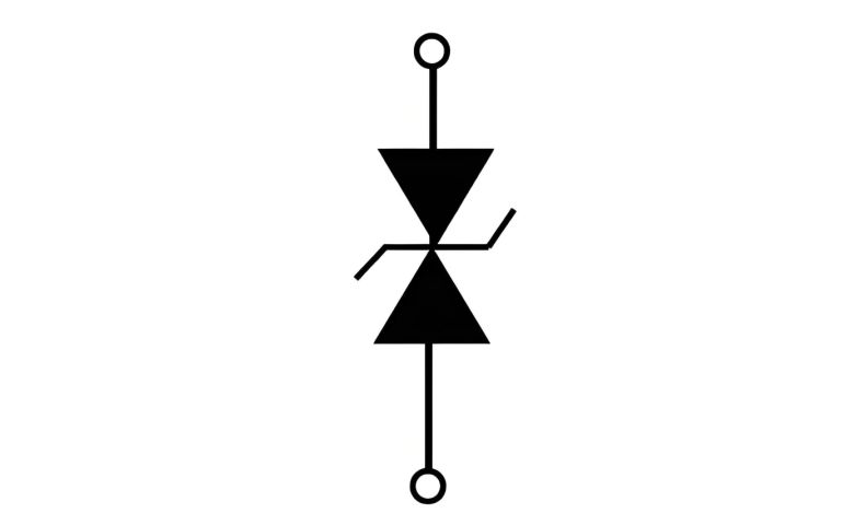
TVS and Zener diodes can both operate in reverse breakdown, but they are optimized for different electrical jobs. A TVS is characterized to divert short transient current and limit residual voltage. A Zener or voltage-regulator diode is characterized for operation in a defined current range over a longer interval. Similar symbols or breakdown voltages do not make the parts interchangeable.
The datasheet reveals the intended job
A TVS datasheet is commonly organized around reverse working voltage, breakdown voltage, clamping voltage, peak pulse current, and peak pulse power. Those parameters describe a device that stays off during normal operation and conducts during a transient.
A Zener or regulator diode datasheet places more weight on regulation current, voltage tolerance, dynamic impedance, power dissipation, and temperature coefficient. It describes a part that may remain in breakdown as part of normal circuit operation.
Before comparing two candidates, inspect which tests the manufacturer publishes:
clamping voltage paired with a pulse current and waveform;
peak pulse power with pulse duration and starting temperature;
continuous dissipation with thermal conditions;
regulation voltage at one or more steady currents;
dynamic impedance in the intended regulation region;
voltage temperature coefficient and allowable junction temperature.
The parameter set is stronger evidence than an informal product label.
VRWM and VBR serve different decisions
Reverse working voltage, VRWM, defines a voltage region in which the TVS remains off within stated leakage conditions. Breakdown voltage, VBR, is measured at a specified test current. The protected circuit's highest continuous voltage should fit within the allowable working region; VBR is not a recommended normal supply voltage.
When a transient forces current through the device, the voltage rises above VBR. Clamping voltage, VC, states the device voltage at a named pulse current under a named waveform. The protected IC is exposed to that clamp plus voltage created by package and PCB inductance.
Read the parameters in this sequence:
Measure or derive the highest valid continuous voltage at the installation point.
Select a working-voltage range that does not create unacceptable leakage.
Check the breakdown range and its test current.
Estimate or measure the transient current through the protection branch.
Compare VC at that current with the downstream limit.
Add temperature, tolerance, and board parasitics before validation.
Replacing VC with VBR in a protection calculation understates the residual voltage.
Peak pulse power is not continuous dissipation
Peak pulse power is established for a specified pulse shape, width, and starting temperature. It does not mean that the diode can dissipate the printed wattage continuously. Repetition rate and thermal recovery also affect how a device handles a sequence.
A sustained overvoltage can hold a TVS in conduction until junction temperature rises beyond its boundary. The eventual failure can be a short, an open path, or a parametric shift. A fuse, electronic switch, current limiter, or overvoltage controller is required when the source can persist. The TVS handles the transient portion while another function terminates the long event.
Continuous regulation requires a steady-state power calculation. The designer must account for diode current, voltage, ambient temperature, thermal resistance, copper area, and allowable junction temperature. A pulse rating cannot replace that work.
The words avalanche and Zener do not define interchangeability
Reverse breakdown can involve Zener tunneling and avalanche multiplication. The dominant mechanism depends on junction design and breakdown region, and practical devices may not fit a simple name-based division. Application engineers do not need to infer semiconductor construction from a catalogue heading.
Use the controlled ordering code and compare the electrical conditions that matter:
maximum continuous reverse voltage and leakage;
VBR range and specified test current;
VC and IPP under the same pulse waveform;
peak pulse power and temperature derating;
continuous dissipation and thermal path;
unidirectional or bidirectional behavior;
package, polarity, footprint, and failure mode.
If the original component lacks a required pulse or continuous rating, do not fill the gap with an assumption based on another diode family.
A regulator diode may fail a transient requirement
A regulator diode can have the correct nominal breakdown voltage yet lack characterized current capability for the source waveform. Its die area, package, thermal path, and surge test may be different. The part could clamp a laboratory signal while suffering damage during the actual pulse sequence.
The inverse substitution also creates risk. A TVS selected for surge energy may have a voltage tolerance, leakage, dynamic impedance, or continuous thermal behavior unsuitable for a precision regulation node. A broad clamping range that is acceptable during a rare transient can be poor regulation during every second of operation.
Validate static operation and transient protection separately
Static validation confirms that the diode does not disturb valid circuit operation. Test supply tolerance, startup, shutdown, hot-plug behavior, line leakage, standby current, and the highest specified temperature. For a regulation circuit, verify voltage and power over its operating current range.
Transient validation confirms current diversion and residual voltage. Use the source defined by the product requirement, then record:
source waveform, impedance, polarity, and event count;
current through the protection branch;
voltage at the diode and downstream sensitive node;
device and board temperature where relevant;
function during and after each event group;
post-stress leakage and breakdown checks.
A result on a component fixture is valuable, but it cannot include the customer's connector, trace, return path, and downstream IC.
Replacement decisions need two boundary checks
The first boundary is normal operation. A candidate must tolerate every valid voltage and temperature without excessive leakage, regulation error, or unwanted conduction. The second boundary is the abnormal event. The candidate must carry the relevant current while keeping the downstream circuit within an accepted voltage and thermal state.
If either boundary is unknown, the devices are not proven substitutes. A matching nominal voltage or package does not close the review.
ASIM organizes TVS selection around those two boundaries. The ASIM TVS diode manufacturer hub provides access to related selection material. Final approval should cite the exact part data, pulse conditions, PCB layout, and product validation record.
A concise engineering rule
Use a TVS when the design problem is short transient energy and residual-voltage control. Use a Zener or regulator device when the circuit intentionally operates in a defined breakdown-current region and the continuous thermal calculation supports it. When one part is proposed for the other's job, repeat both the static and transient analysis rather than approving it by voltage name.
TVS and Zener Selection FAQ
Can a Zener diode replace a TVS with the same breakdown voltage?
The voltage match is insufficient. The Zener must also have suitable pulse-current, waveform, clamping, thermal, package, and post-stress behavior for the transient source.
Can a TVS diode regulate a voltage continuously?
A TVS may conduct near breakdown, but continuous regulation requires a current, tolerance, dynamic-impedance, and thermal analysis. A pulse rating does not establish continuous capability.
Why is clamping voltage higher than breakdown voltage?
VBR is measured at a specified low test current. VC is measured while a much larger transient current flows, so dynamic resistance and parasitic inductance raise the observed voltage.
 Previous