Submit






Author: ASIM Technical Team | Published: 2026-09-12
GB/T 4937.28-2026 took effect on September 1, 2026. Its scope is charged-device-model, or CDM, electrostatic-discharge sensitivity testing for semiconductor devices. That scope matters: a CDM classification describes a device-level event. It does not certify a finished product against a user-generated electrostatic discharge.
HBM, CDM, and system-level ESD are often compressed into one line in a component approval form. The result looks convenient but removes the information an engineer needs. Each test has a different object, source network, current path, and use. A product can contain a component with a documented CDM classification and still reset during a discharge to its enclosure. An ESD diode can survive a stated IEC pulse in a component test while the protected IC sees excessive residual voltage on the assembled PCB.
What the new standard actually covers
CDM represents a semiconductor device that becomes charged and then discharges rapidly when one terminal contacts a low-impedance path. The device under test is normally an unpackaged or packaged semiconductor component, not an operating end product with a cable, enclosure, display, and complete PCB.
The information supports device handling, assembly controls, qualification, and failure analysis. It can help a quality team answer questions such as whether a device needs tighter electrostatic controls during storage or placement. It cannot answer whether a customer touching a metal button will disturb the product.
The title of GB/T 4937.28-2026 identifies the boundary: semiconductor devices, ESD sensitivity testing, charged device model, device level. A record that says only “ESD passed” omits the most important part of the result.
Three tests, three engineering questions
| Test category | Typical object under test | Event being represented | Main use of the result |
|---|---|---|---|
| CDM | semiconductor device | a charged device rapidly discharges through a terminal | device sensitivity classification and process control |
| HBM | semiconductor device | a charged human-body model discharges into a device terminal | device sensitivity classification and handling control |
| system-level ESD | complete equipment or subsystem | a user or external object discharges to an accessible point | product immunity and functional-performance assessment |
The current waveforms are not interchangeable. CDM has a very fast leading edge, and package inductance can strongly affect the internal stress. HBM uses a defined source network to apply a different device-level event. A system-level test includes the enclosure, connector shells, cables, PCB return path, software state, power system, and every coupling route between them.
This is why a voltage number without a model is incomplete. “2 kV CDM,” “2 kV HBM,” and “2 kV contact discharge” do not describe equivalent stresses.
Why a strong CDM rating cannot prevent a system reset
Suppose a finished unit resets when a discharge is applied to a metal seam. The current may first enter the chassis, flow through a shield connection, mounting screw, cable braid, or I/O ground, and then create a common-mode voltage across the PCB. The disturbed signal could be RESET, a crystal node, an interrupt line, a power supervisor, or a communication reference. The suspected IC may never experience an event resembling its component CDM test.
The device-level result remains useful, but it answers a different question. It tells the manufacturing and quality teams about component sensitivity. The system test must still be performed at specified accessible points, polarities, event counts, and operating modes. Monitoring should include supply rails, reset cause, critical communications, and any function used to define the performance criterion.
At minimum, the system record should preserve:
the physical discharge point and discharge mode;
polarity, level, event count, and interval;
cable, load, firmware, and operating state;
the observed waveform, functional response, and recovery action.
An ESD diode rating is not a product certificate
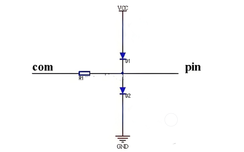
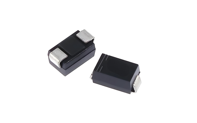
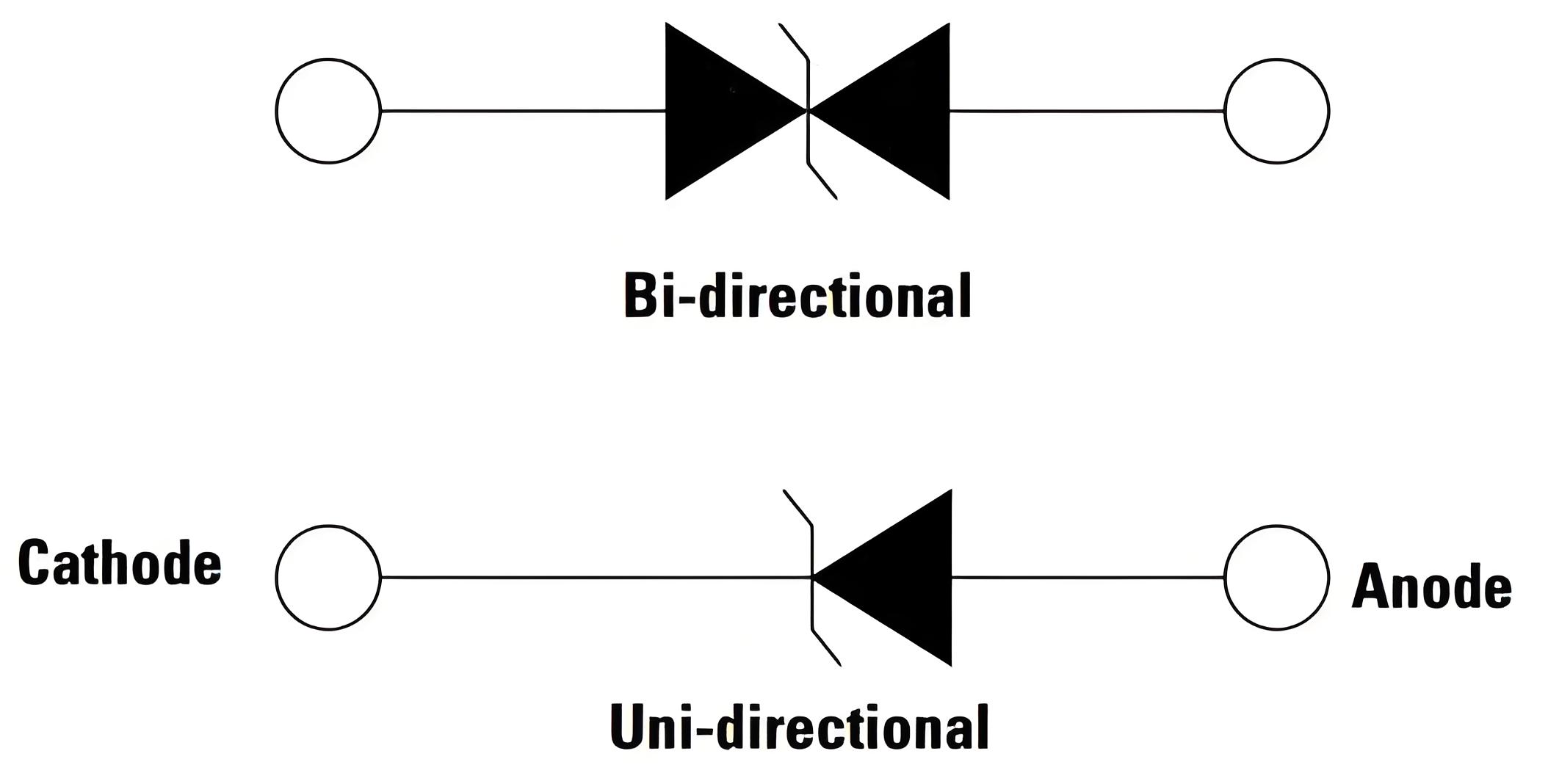
An ESD protection diode is commonly characterized under an IEC 61000-4-2 pulse using a defined fixture and terminal arrangement. That result is valuable for screening protection devices. It does not establish that the assembled product will achieve the same test level.
At board level, the protected IC can see more than the voltage measured across the diode. A useful first-order description is:
IC-side stress ≈ diode clamp voltage + voltage across the discharge-path inductance + local ground shift
The inductive term grows with current slew rate. A long branch from the connector to the diode, a via-heavy return, or a path that shares impedance with the IC ground can therefore defeat an otherwise suitable device. Package choice, pin assignment, placement, return geometry, and the measurement location belong in the same decision as the datasheet clamp value.
Keep four evidence sets separate
A review is easier when it does not attempt to create one universal “ESD level.” Keep these records in separate fields:
the component CDM and HBM classifications, including the test method used;
the protection diode's VRWM, VBR, VC, capacitance, leakage, pulse condition, and terminal configuration;
the applicable system-level standard, discharge mode, point, polarity, event count, operating state, and performance criterion;
the assembled-board waveform or monitored behavior at the protected IC and critical power or reset nodes.
This separation also prevents a common procurement error. A supplier comparison should not rank components by the largest isolated voltage printed on the first page. The comparison must use equal test conditions and must retain the waveform, current, temperature, fixture, and acceptance criterion attached to each number.
How to apply the distinction in a new design
When the IC is selected, place its HBM and CDM information in the component-quality record. Use that information for receiving, storage, assembly, and process-control decisions.
During PCB design, create a separate port inventory. List connector pins, shells, buttons, touch points, exposed conductors, seams, and cables. For each point, identify the likely entry path, the sensitive circuit, the intended shunt or shielding path, and the node that must be monitored during verification.
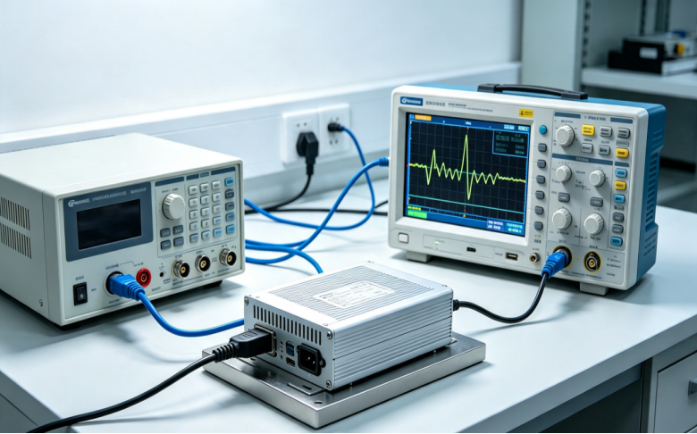
After prototypes arrive, test the complete unit with representative cables, loads, firmware, and operating modes. If a failure occurs, classify the symptom before changing components: power interruption, reset, communication error, latch-up, false trigger, or permanent damage. That classification directs the investigation toward the relevant current path.
ASIM maintains an ESD diode manufacturer and selection page for component and application information. A manufacturer page can narrow the candidate set, but final approval still requires the complete part number, controlled datasheet conditions, PCB implementation, and measured product behavior.
Review language that remains technically valid
Avoid statements such as “the IC has high CDM immunity, so no system protection is required” or “the diode passes ±8 kV, so the product passes ±8 kV.” A defensible record is more specific: “Device-level CDM and HBM information has been reviewed; accessible product ports remain subject to system-level verification under the applicable test plan.”
The sentence is less dramatic, but it preserves the boundary of the evidence. That boundary is what makes the result usable in design reviews, supplier approvals, and later failure analysis.
CDM, HBM, and System ESD FAQ
Does GB/T 4937.28-2026 replace system-level ESD testing?
No. It addresses device-level CDM sensitivity. A finished product must still be assessed under its applicable system or product-level requirements.
Can CDM and HBM voltage classifications be compared directly?
No. They use different models and waveforms. Retain the method and classification with the voltage value.
Why can the IC-side voltage exceed the diode clamp voltage?
PCB and package inductance, shared return impedance, and local ground movement add voltage during a fast current transient. The measurement location therefore changes the observed result.
Original Publisher: Shenzhen ASIM Electronics Co., Ltd.
Copyright notice: Copyright belongs to Shenzhen ASIM Electronics Co., Ltd. Please retain the author, source, and original URL when quoting or republishing.
Original URL: https://asim.com.cn/gb-t-4937-28-2026-cdm-hbm-system-esd-en.html
 Previous