





 Submit


How should the design be rectified if the power port fails the surge test?
 2026.07.17 00:00:00
 83
83





If a power port fails the surge test, a systematic review should be conducted covering the TVS working voltage (VRWM), clamping voltage (VC), peak power and current-handling capability, package selection, upstream current limiting, ground loops, and PCB trace layout. Remediation efforts must go beyond simply checking whether the TVS has burned out; it is crucial to determine whether surge energy has bypassed the protection device and entered downstream circuitry.
I. Common Failure Phenomena
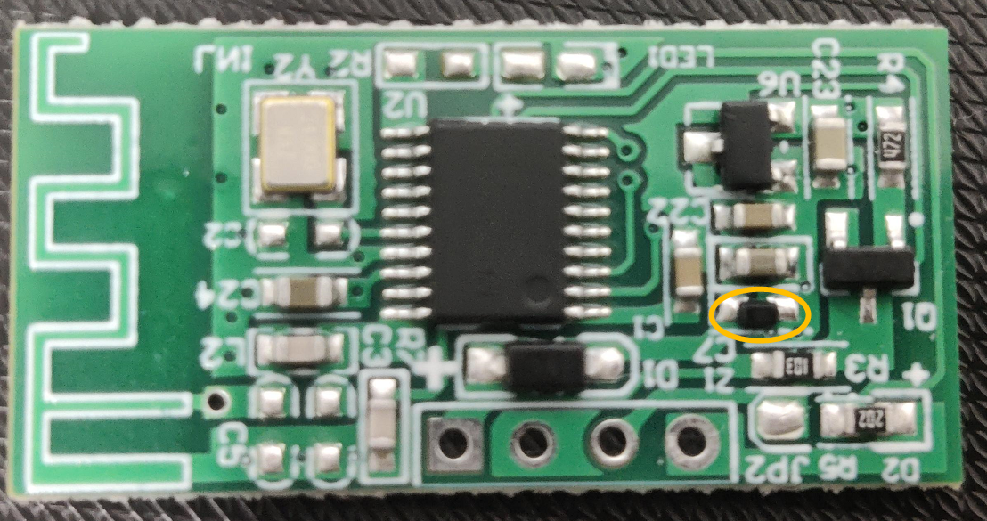
Surge failures at the power port can manifest as a blown fuse, TVS breakdown (short circuit), DC-DC converter damage, system reboot, MCU lock-up, damage to downstream chips, or functional anomalies following the test. Different phenomena indicate distinct issues regarding energy absorption, clamping voltage, voltage withstand margins, or discharge paths. Actual testing has revealed various failure modes: an MCU power pin shorting to ground under surge impact; downstream circuitry sustaining damage due to excessive clamping voltage despite the original TVS remaining intact; and the breakdown of a downstream MOSFET in a charging dock under high-level surges. These examples demonstrate the diversity of failure modes, necessitating targeted analysis.
II. Check TVS Parameters First
VRWM (Reverse Working Voltage / Standoff Voltage): If too low, it may trigger false conduction during normal operation; if too high, clamping may occur too late. Selection should be based on the normal operating voltage.
VC (Clamping Voltage): Excessive clamping voltage exposes downstream components to overvoltage, potentially damaging the downstream chip.
Peak Power and Current Handling Capability: Insufficient power rating leads to TVS failure; generally, higher current handling capability combined with lower clamping voltage yields better performance.
Package and Junction Capacitance: Packages that are too small may fail to withstand test energy levels and can restrict PCB layout; junction capacitance selection depends on the port type (e.g., low capacitance is not strictly necessary for 5V power lines, but signal lines require careful consideration of potential signal degradation).
Consider Actual Waveforms and Standards: Component selection must be based on standard test waveforms—such as the 1.2/50μs combination wave (paired with an 8/20μs current wave and 2Ω source impedance)—rather than relying solely on nominal voltage ratings or incorrectly using non-standard waveforms.
III. Re-examine PCB and System Paths
The TVS should be placed close to the power input, adhering to the "protection before filtering" principle; primary protection components must precede filtering components to prevent the latter from being damaged by surges. Return paths should be short and wide, and the ESD discharge ground should be robust. If surge current passes through narrow, long traces or sensitive areas, it may cause system resets or chip damage.
Placement and Layout: The TVS should be positioned near the interface; for multi-node protection, devices can be placed near the corresponding pins or main lines at the MCU power input, cable end, and charger end.
Grounding Optimization: Optimizing the grounding layout can significantly enhance surge immunity and reduce interference with internal circuitry.
When necessary, incorporate upstream current limiting, fuses, or common-mode filtering, or optimize the connection between the chassis ground and the system ground.
IV. Asaim Remediation Support
Asaim can recommend TVS package, power rating, and layout remediation solutions based on the customer's test level, schematics, PCB design, and failure phenomena, and verify these solutions through EMC laboratory testing.
FAQs
Q: Does a burnt-out TVS indicate incorrect component selection?
A: It could be due to insufficient power rating, a lack of current limiting in the preceding stage, or a poorly designed surge path. Additionally, a TVS might remain intact yet allow a clamping voltage high enough to damage downstream components; therefore, one cannot judge the situation solely by the TVS's physical appearance.
Q: Will switching to a larger package guarantee passing surge tests?
A: Not necessarily. Success also depends on the clamping voltage, grounding integrity, and PCB trace routing.
Q: Where should the TVS for a power port be placed?
A: It should generally be placed near the power input and upstream of the filtering components (protection before filtering); the earlier the surge energy is diverted, the better the downstream circuitry is protected. For multi-node protection, TVS devices can be placed near the relevant pins or main lines at the MCU power input, the cable end, and the charger connector.
 Previous

Related News
2026.06.18
ESD Protection for HDMI and DisplayPort Interfaces: 4K/8K Video Connector Design Guide
2026.06.22
ESD Diode vs TVS Diode: Which to Use and When
2026.07.11
How is the ESD0524 series used for USB interfaces?
2026.07.11
How do you design an ESD protection scheme for USB interfaces?
2026.07.13
How should ESD protection devices be laid out for a Type-C port?
2026.07.13
How do I select a 5V low-capacitance ESD diode model?
2026.07.13
What should be done if a USB interface fails ESD testing?
2026.07.15
For what applications are SOD-323 packaged ESD diodes suitable?
2026.07.15
How do you select a low-capacitance ESD protection device for an HDMI interface?
2026.07.16
How do you design a surge protection solution for industrial power supplies?


