





 Submit


How should ESD protection devices be laid out for a Type-C port?
 2026.07.13 00:00:00
 88
88





The core principles for the layout of ESD protection devices for Type-C interfaces are: proximity to the connector, short discharge paths, symmetrical high-speed signal lines, and an intact ground return path. Given the large number of signal lines in a Type-C interface, protection devices cannot simply be placed near the main controller; protection schemes and layouts for CC, SBU, USB 2.0, high-speed differential lines, and VBUS must be designed individually based on their respective functions.
I. Why is the Type-C interface more challenging to lay out?
Type-C connectors support reversible plug-in and contain multiple sets of high-speed signal lines, as well as CC, SBU, D+, D-, and VBUS lines. Since each type of line has different requirements regarding voltage, data rate, and noise immunity, the placement of ESD protection components must be handled in accordance with the interface definition.
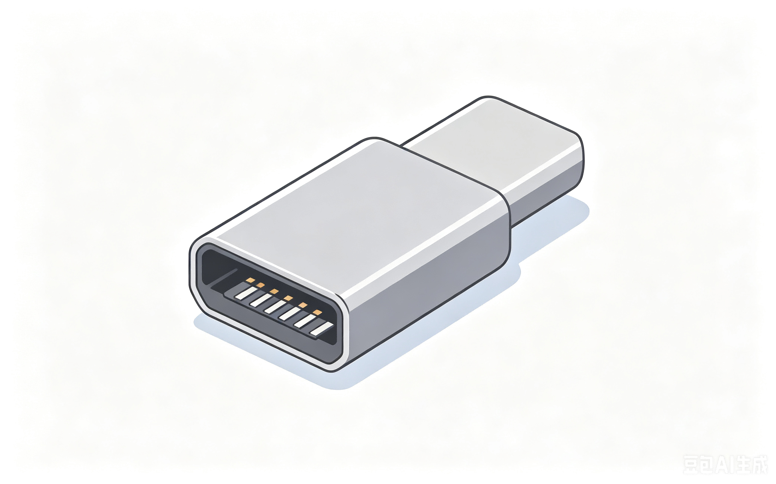
If all protection components are placed far away from the connector to save space, electrostatic energy will first enter the board's traces, resulting in reduced protection effectiveness.
II. Placement Principles for Different Signal Lines
For high-speed differential lines, ESD protection components should be placed close to the connector while maintaining left-right symmetry; avoid unnecessary branches and impedance discontinuities. Low-capacitance components may be used for D+ and D- lines. Appropriate protection devices should be selected for CC and SBU lines based on protocol specifications and the risk of abnormal voltages, while power surges should be the primary consideration for VBUS lines.
The GND terminal of the protection device should be connected to ground via a nearby via rather than routed through a long, thin trace to a distant ground point. The grounding method for the connector housing also affects the ESD discharge path.
III. Common Layout Pitfalls
Common issues include placing ESD devices too far from the interface, positioning vias too far from GND pins, using excessively long branches for high-speed differential lines, asymmetrical layout of left and right channels, and sharing unsuitable protection devices between VBUS and high-speed lines.
These issues can lead to unstable ESD test results, USB recognition failures, malfunctions in fast-charging protocols, or signal attenuation in high-speed communications.
IV. Asym Recommendations
Based on the various functions of the Type-C interface—such as USB 2.0, USB 3.0, PD fast charging, and audio multiplexing—Asym offers recommendations for low-capacitance ESD protection, ESD arrays, power-rail TVS, and EMI filtering solutions.
FAQs
Q: Does every Type-C line require ESD protection?
A: Critical signal lines that are externally accessible or located near the interface generally require ESD protection; the specific number of lines protected depends on product functionality and testing standards.
Q: Can the ESD device be placed near the main controller?
A: This is not recommended. Placing it close to the interface is more effective for discharging static electricity before it enters the board.
Q: How should I select ESD protection for Type-C high-speed lines?
A: Prioritize components with low junction capacitance and low-parasitic packaging that are suitable for differential pair routing.
 Previous

Related News

2024.10.12
EMC testing Contents and Current Situation of Automotive Electronic products

2025.02.21
How to choose the best circuit protection devices in a circuit?
2025.09.08
High-frequency Circuit TVS Diode Junction Capacitance Optimization Strategy -ASIM
2025.09.10
The Function and Working Principle of MOSFETs -ASIM

2025.11.17
What is an eye diagram? A comprehensive guide to the function and principle of eye diagrams - ASIM Electronics
2026.06.11
ESD Protection for High-Speed Automotive Interfaces
2026.06.22
ESD Diode vs TVS Diode: Which to Use and When
2026.07.10
What is the difference between SMD TVS and leaded (through-hole) TVS?
2026.07.11
How is the ESD0524 series used for USB interfaces?
2026.07.11
How do you design an ESD protection scheme for USB interfaces?


