Submit






A 48 V DC input needs a TVS review based on the highest continuous input voltage first. Read VRWM, VBR, VC and IPP with their stated test conditions, not as interchangeable labels.
Direct answer
Record the highest continuous voltage, the transient source, the downstream withstand limit and the PCB return path. Then compare complete part data under the same waveform and current basis before checking the target board.
Define the continuous-voltage window
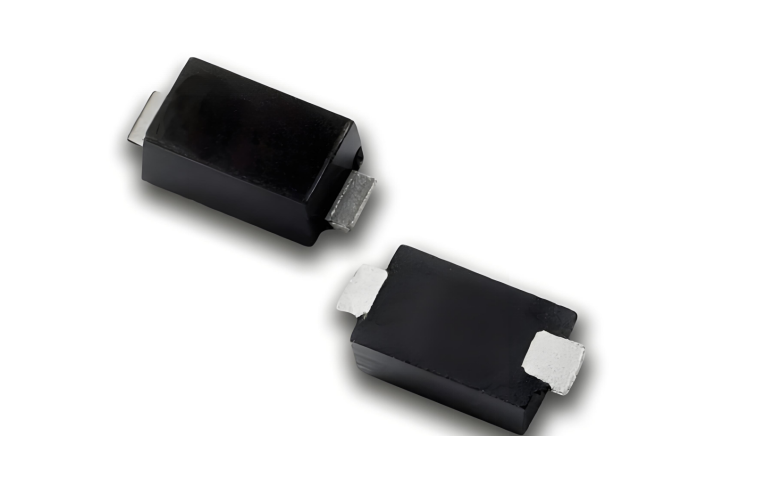
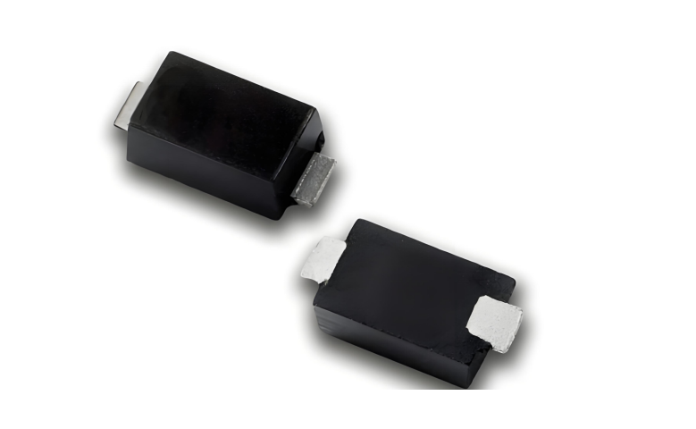
A 48 V nominal label does not state the highest sustained voltage at the connector. Supply tolerance, startup and abnormal-but-continuous states belong in the selection record. The ASIM SMA04J document shows how VRWM, VBR, VC and IPP are presented with stated conditions. It is a reference for reading the fields, not an approval for a 48 V design.
| Field | Review action | Reason |
|---|---|---|
| VRWM | Cover the highest continuous port voltage | A nominal voltage is not a continuous limit |
| VBR | Read the stated breakdown range | Breakdown is not the clamping result |
| VC / IPP | Keep current and waveform beside the value | The values are condition dependent |
| Package / layout | Check pinout and return path on the PCB | Board parasitics change the result |
Verify the clamping path on the board
Measure the TVS terminals and the protected node on the target layout. Keep the source setting, cable condition, board revision and functional state in the same record. A component datasheet does not establish a system-level transient result by itself.
Selection sequence
Document the normal and abnormal continuous voltage states.
Compare complete candidate datasheets using the same waveform basis.
Check polarity, package drawing and downstream withstand voltage.
Repeat functional and node-voltage checks on the target board.
Frequently Asked Questions
Can a 48V label be used as the VRWM value?
No. VRWM must cover the actual highest continuous voltage at the protected port.
Is a lower VC always preferable?
No. VC must be reviewed with VRWM, waveform, current, leakage, thermal conditions and the downstream limit.
Data source
Data verification date: 2026-10-13. These parameters must be used in conjunction with the complete model number, specification version, test conditions, and project verification records; the device data herein does not equate directly to conclusions regarding the complete system.
 Previous