





 Submit


How to Read ESD Diode Capacitance for High-Speed Interfaces
 2026.08.06 00:00:00
 87
87





An ESD diode appears as a shunt capacitance on a signal line while it is not conducting. That load is often secondary on a pushbutton or low-speed GPIO, but it can increase insertion loss, disturb impedance, and reduce eye opening on USB, HDMI, MIPI, or Ethernet links.
A catalog value such as 0.2 pF is not a complete channel model. Test frequency, DC bias, temperature, package parasitics, and whether the value applies to one channel or an entire array all affect how the number should be used. Selection begins with the interface budget, not with the lowest value in a product table.
What does the Cj value represent?
Cj normally represents the effective junction capacitance measured at a specified frequency and bias voltage. An ESD protection junction is nonlinear, so its capacitance changes with reverse bias. Many tables show a typical value; a high-speed design also needs to consider maximum value and production spread.
Test frequency matters because the measurement includes different parasitic effects as frequency rises. Two devices measured under different conditions should not be ranked solely by their headline values. At multi-gigahertz frequencies, package inductance, pad capacitance, and fixture de-embedding can be as important as the semiconductor junction.
Bias voltage changes depletion width. Junction capacitance commonly falls as reverse bias increases. A value measured at 0 V can therefore differ from one measured at 2.5 V even when the underlying devices are similar. Always compare the measurement conditions.
Does lower capacitance guarantee a better high-speed protector?
A single Cj value does not describe the whole channel
A differential channel contains device capacitance, package inductance, PCB pads, vias, stubs, and reference-plane transitions. The resulting insertion loss and return loss come from the full network.
The ASIM ESD5E001TA is a bidirectional 5 V device with a typical junction capacitance of 0.08 pF in a DFN0603-2L package. The ESD5E003TA is also a bidirectional 5 V device, with a typical capacitance of 0.3 pF. The lower-capacitance option places less nominal load on the line, but pulse current, clamping voltage, board assembly, and package handling still belong in the decision.
Channel matching matters on differential pairs
Unequal loading between the positive and negative conductors converts part of the differential signal into common-mode energy. An array should offer suitable channel matching, and the PCB fanout should remain symmetrical. Two discrete devices with the same nominal Cj can still produce imbalance through pad or stub differences.
Protection performance still has to pass
Very low capacitance is not useful if the residual voltage exceeds the interface IC's tolerance. The ASIM ESD5D002SA, for example, has a 5 V VRWM, typical Cj of 0.2 pF, peak pulse current of 8 A, and maximum clamping voltage of 12 V under its stated condition. Those parameters let the engineer examine both loading and protection rather than optimizing only one side.
How should a capacitance budget be set?
For a low-speed control line, begin with working voltage, leakage, and clamping voltage, then verify that added capacitance does not slow the edge beyond the logic margin. For a high-speed serial link, start from the channel model, loss budget, and eye mask. Allocate a portion of that budget to the connector, traces, vias, ESD device, and receiver package.
MIPI D-PHY and high-speed USB links have short unit intervals and can be sensitive to a small impedance discontinuity. Ethernet requires an additional topology decision: a protector on the PHY side of the isolation transformer sees a different common-mode environment from one on the cable side.
Multi-channel arrays can shorten routing and improve matching. The ASIM ESD5Z004SR08 is a 5 V unidirectional low-capacitance array with a typical 0.3 pF Cj in a DFN2510-10L package. The ESD5X004SA is a 5 V bidirectional array with a typical 0.25 pF Cj in a DFN2010-5L package. Channel count, internal connections, and pinout should be checked against the connector before layout begins.
How much capacitance does the PCB add?
Place the protector close to the connector
Short placement reduces the unprotected trace length and avoids creating a long open stub. Routing the high-speed pair past the protection point and then branching to the diode weakens both ESD performance and signal integrity.
Keep pads proportionate to the package
An ultra-small device mounted on oversized pads, long neck-downs, or large test points can acquire board parasitics comparable to its stated Cj. Use the recommended land pattern and preserve a continuous reference plane.
Give discharge current a short return
The diode's return should reach chassis ground or the intended discharge reference through a short, wide path. A remote return via adds inductance and raises the residual voltage. Do not cut the high-speed reference plane near the protection footprint.
How should the selected part be verified?
Build a controlled comparison with no protector, candidate A, and candidate B. Keep the board, cables, and instrument settings constant. Measure the relevant parameter: insertion loss and return loss, eye height and width, jitter, or bit-error rate.
Repeat the check across expected cable and temperature variation. A clean waveform at room temperature on one short cable is not a production limit.
Then perform ESD testing and observe the residual transient near the protected IC. Signal-integrity and immunity tests should use the final placement and return path. A flying-wire sample does not represent the parasitics of a production PCB.
Common questions
Can a typical Cj value be treated as the worst case?
No. A typical figure represents a common device, not the upper production limit. Ask for a maximum value, distribution information, or validate multiple lots when the channel margin is small.
Is 0.5 pF automatically too high for a fast interface?
No. Data rate, package, footprint, channel length, and receiver margin determine the result. Channel simulation or an eye-diagram test is more useful than a universal capacitance cutoff.
Is array capacitance specified per channel or for the whole device?
Datasheet conventions vary. Check the parameter definition and internal schematic to determine whether the value applies to one line, a line pair, or a shared node.
Does lower capacitance always mean a lower ESD rating?
No fixed relationship applies, although low capacitance, low clamping voltage, and high pulse current require design tradeoffs. Compare devices using the same standard and waveform.
A useful selection table includes Cj test conditions, VRWM, VC, IPP, package, channel matching, and board-level results. That is a more reliable definition of a low-capacitance solution than the catalog value alone.
 Previous

Related News

2024.10.12
EMC testing Contents and Current Situation of Automotive Electronic products

2025.02.21
How to choose the best circuit protection devices in a circuit?
2026.07.24
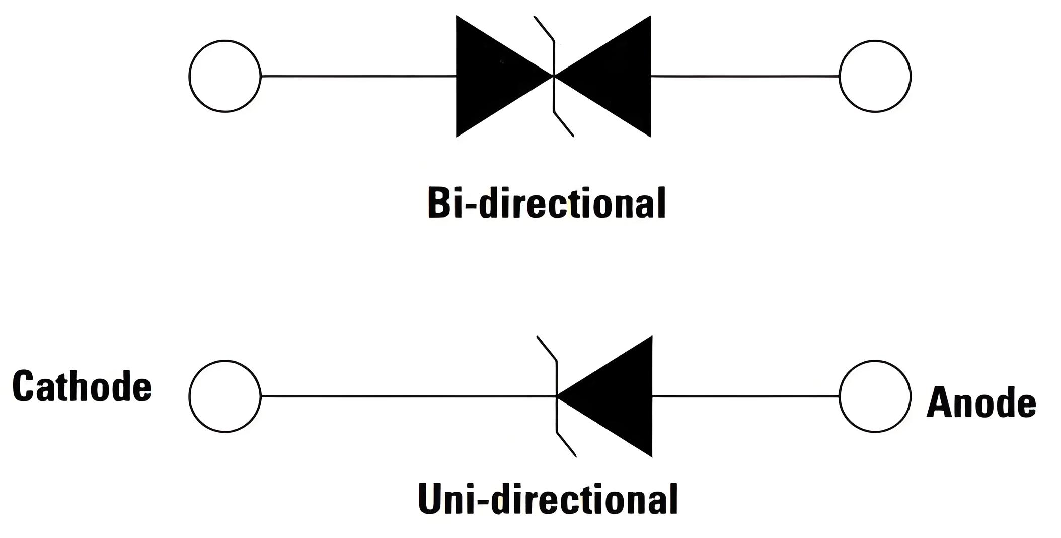
How to Choose Between Unidirectional and Bidirectional TVS: A Comparison of DC Power Supplies, AC Signals, and Communication Interfaces
2026.07.29
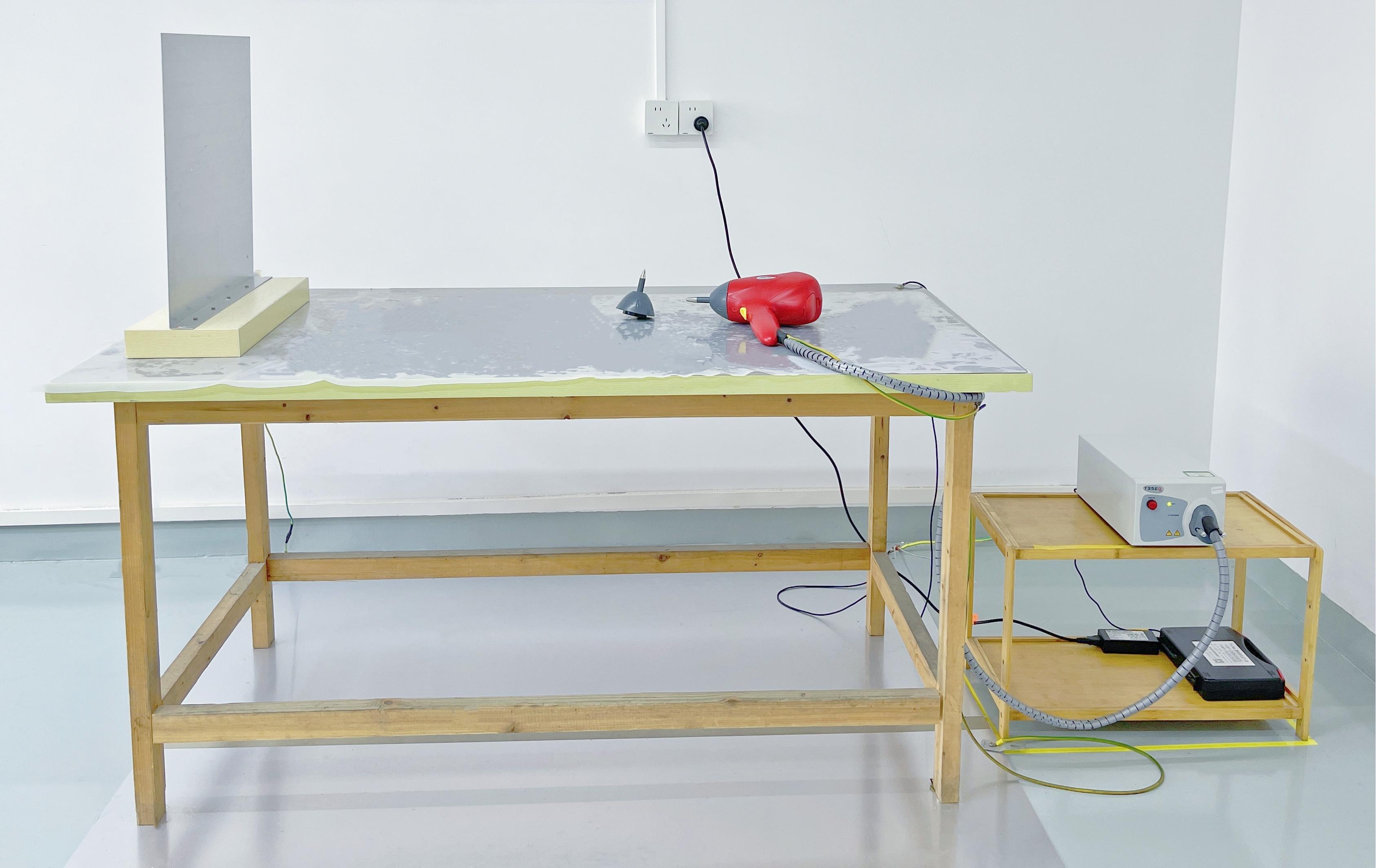
Why does the ESD test still fail after replacing the protection device? Troubleshooting discharge paths, grounding, and component placement.
2026.08.04
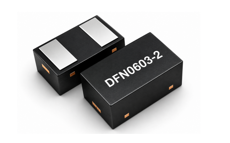
How to handle an MCU reset pin susceptible to ESD interference? Checking RC circuits, supervisory chips, and PCB traces.
2026.08.04
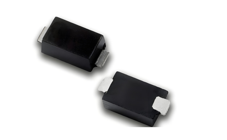
How to implement ESD remediation for devices with plastic housings? Design considerations for buttons, cutouts, and internal PCB dimensions.
2026.08.05
How to Read TVS Diode Reverse Leakage Current (IR): Temperature, VRWM, and Standby Power
2026.08.05
How to Read IEC 61000-4-2 Ratings for ESD Diodes: Component Rating vs System Compliance
2026.08.05
How to Read TVS Diode Peak Pulse Power: Waveform, Temperature, and Pulse Width A 200 W, 600 W, or 1500 W rating on a TVS diode is peak pulse power under a defined waveform and starting temperature. It is not continuous power dissipation. PPPM must be read together with pulse width, waveform, peak pulse current, clamping voltage, and thermal derating. The same TVS can tolerate very different peak currents for a short, fast pulse and a longer surge. Unless the test conditions match, a 1500 W dev
2026.08.06
Why TVS Diodes With the Same VRWM Have Different Clamping Voltages


