Submit






A POS terminal combines user-accessible touch surfaces, plug-in data ports, card contacts, network cabling, and a DC input. These nodes do not share one electrical protection requirement.
Short answer: Record the actual voltage, bandwidth, capacitance budget, and protected-IC tolerance for every exposed path. Screen touch and high-speed data lines for low loading, evaluate the SIM interface pin by pin, and treat the DC input and Ethernet path separately. Place protection at the external entry with a short return path.
Build a requirement table for each exposed interface
| Interface | Normal condition | Primary selection constraint | Board-level check |
|---|---|---|---|
| Touch FPC | I²C, SPI, or touch-specific signals | VRWM, capacitance, leakage | Touch accuracy and recovery |
| USB D+/D− | High-speed differential data | Low capacitance, S-parameters, symmetry | Enumeration and eye margin |
| SIM socket | VCC, RST, CLK, I/O | Voltage range, topology, leakage | Card recognition and timing |
| Ethernet | Magnetics and PHY path | Location, capacitance, common mode | Packet loss and reconnect |
| DC input | Adapter and cable transients | VRWM, VC, pulse capability | Start-up and thermal behavior |
The validation state should include payment processing, network traffic, printing, card activity, and idle operation. A unit that stays powered but loses a transaction or link has not met a functional immunity criterion.
Four boundaries to verify before approving a device
1. Working voltage
Measure the highest normal value, tolerance, and start-up overshoot on each node. A label such as “3.3 V system” is not a substitute for the waveform at VCC, clock, reset, data, and power-entry pins.
2. Capacitance and signal bandwidth
USB and touch data lines are sensitive to device and layout capacitance; the SIM clock also has an edge-rate constraint. Low capacitance is not a universal objective for the DC input, where clamping and pulse capability usually dominate.
3. Clamping data and its test condition
Compare clamping voltage only when current, waveform, and pulse duration are stated. An 8/20 μs point, a TLP curve, and an IEC 61000-4-2 rating are not interchangeable.
4. Package, placement, and return path
Route each exposed signal to the protection element before the protected IC. Keep differential branches balanced, place card protection close to the socket, and define whether the shield returns to chassis or circuit reference.
A repeatable board-validation sequence
Freeze enclosure, cables, adapter, firmware, and operating state.
Map every exposed metal point and connector gap.
Capture reset, power, USB, network, and application logs during each discharge.
Change one device, return path, or structural variable at a time.
Repeat touch, card, payment, printing, network, and thermal regression tests.
How ASIM public data can support candidate screening
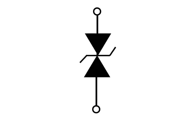
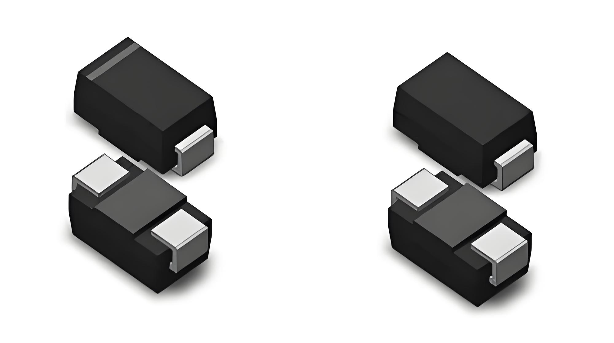
ASIM publishes ESD5E001TA with a 5 V class, DFN0603-2L package, and 0.08 pF typical junction capacitance, making it a starting candidate for low-loading lines. ESD3V3D500TA publishes ±3.3 V VRWM, 50 pF typical capacitance, and 8/20 μs clamping points for a different class of node. These parts should not be interchanged solely by brand or package.
Traceable numbers make a comparison auditable. They do not replace testing on the target assembly, and a component ESD rating must not be presented as the immunity level of the finished product. IEC 61000-4-2 defines the system-level test method; the applicable product standard and test plan determine levels and performance criteria.
Questions engineers often ask
Can one 3.3 V ESD diode protect every 3.3 V signal?
No. Bandwidth, leakage, capacitance budget, default state, and protected-pin tolerance remain different.
Does a ±15 kV component rating guarantee a ±15 kV terminal?
No. The enclosure, PCB, cables, return path, and operating state determine the finished-product result.
Should protection be placed close to the processor?
It is generally more effective at the external entry so current is diverted before it travels through the board.
 Previous