





 Submit


ESD5X004SA: 5 V Bidirectional ESD Array Design Review
 2026.08.21 00:00:00
 52
52





ESD5X004SA is an ASIM bidirectional ESD array in a DFN2010-5L package. The verified values are 5 V reverse working voltage, 6 V minimum breakdown, 6 A maximum peak pulse current, 12 V maximum clamp voltage, and 0.25 pF typical junction capacitance. The package and several headline values resemble the 3.3 V version, but the normal operating window is different and must be reviewed before any substitution.
Draw the complete 5 V power-state timeline
A signal labelled 5 V does not remain in one state throughout the product lifecycle. The external equipment may be powered while the local board is off. The line can ramp slowly during startup, remain high during shutdown, or receive an unexpected level through a remote pull-up. These states affect leakage and back-powering before ESD performance is considered.
Record at least these conditions for every proposed channel:
the highest and lowest voltage during normal communication;
the local-power-off and remote-power-on state;
startup, shutdown, hot-plug, and standby behavior;
any negative swing or AC-coupled operation;
the role of the shared reference connection.
The 5 V working window makes ESD5X004SA a logical candidate for appropriate 5 V signals. It does not make the array suitable for a supply rail that must absorb long-duration surge energy, nor for a line with a negative swing outside the device boundary.
Compare the 5 V and 3.3 V versions by operating window
ESD5X004SA and ESD3V3X004SA are both bidirectional DFN2010-5L arrays with 0.25 pF typical capacitance, 6 A maximum peak current, and 12 V maximum clamp voltage. Their working and breakdown windows differ: ESD5X004SA is 5 V with 6 V minimum breakdown, while ESD3V3X004SA is 3.3 V with 4.2 V minimum breakdown.
Use the following decision sequence:
Exclude the 3.3 V version if any normal state exceeds its working boundary.
Do not choose the 5 V version merely because it sounds more universal.
Compare the receiver limit with the clamp condition and PCB overshoot.
Confirm leakage and signal behavior during powered-off states.
Validate the selected array on the implemented board.
The equal 12 V clamp figures do not make the two parts interchangeable. Normal-operation compatibility comes before transient comparison.
Assign channels by role instead of spare capacity
Four exposed lines can share an array when voltage, polarity, direction, capacitance, and failure isolation are compatible. A bidirectional data line, a supply-sense input, and a safety-related control line may all fit within 5 V yet still be poor candidates for one shared structure. Review what happens if one channel is disturbed and the common node moves.
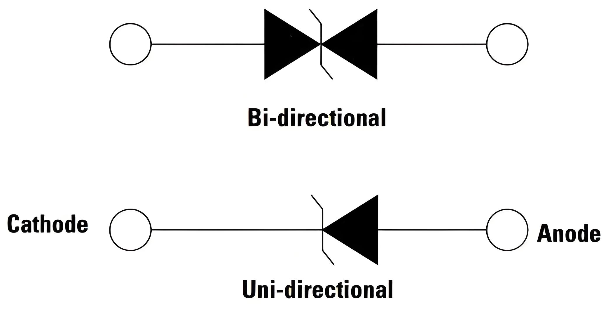
The bidirectional structure is useful for signals that require a blocking window in both polarities. It is not a universal answer for unipolar supply rails. Power inputs need a separate energy and clamp review, including continuous current and long-pulse heating.
Document the connector pin, array channel, and receiver pin in one table. This prevents a future PCB revision from silently moving a different voltage domain onto an unused channel.
Route each signal through the protection area
Install the DFN2010-5L array near the connector entry. Each exposed signal should encounter the protection pad before traveling into the board. Avoid long T-branches, because the branch becomes a high-frequency load and leaves part of the internal route exposed before the protection current can turn toward the reference plane.
Keep the common reference connection short and wide. A narrow neck shared by all four channels produces common inductance and can transfer disturbance between nets. Review reference-plane continuity under the connector and array, especially when the interface crosses a split or changes layers.
For fast lines, compare branch length and via count between channels. Equal device capacitance does not preserve symmetry when the PCB fanout differs.
Separate leakage testing from stress testing
Measure normal line levels, standby current, startup, shutdown, and communication before the ESD sequence. A design that passes one discharge point but creates powered-off leakage or alters an input threshold has not completed the review. Keep an original assembly for A/B/A comparison.
Use the same cable, external equipment, firmware, supply, and load for each comparison. Record errors, recovery, and the apparent interface state. For wake, reset, or interrupt lines, save event counters and timing. For data lines, use the target operating mode rather than a reduced bench rate.
The release package should include:
device marking, datasheet revision, and board footprint;
line-to-channel mapping and the common return location;
normal and powered-off current measurements;
functional results before and after installation;
target stress configuration and recovery observations.
After the first successful board, repeat the review on more than one assembly when the project risk requires it. Array behavior can be affected by connector tolerance, solder geometry, and a return via that is partially obstructed by another layout change. A second board also helps separate a repeatable design result from an accidental cable or bench condition. Keep rejected candidates in the review table with a short reason, such as excessive powered-off leakage, an incompatible pin map, or a branch that could not be routed symmetrically. That record is more useful than a list containing only the selected part number.
Questions about ESD5X004SA use
Is ESD5X004SA suitable for every 5 V interface?
No. The interface must also fit the bidirectional topology, capacitance, channel mapping, receiver limit, and powered-off behavior.
What does the 12 V clamp value mean?
It is the maximum device-terminal clamp at the stated 6 A condition. PCB inductance can make the voltage at the receiver different.
When should the array be revalidated?
Revalidate when the connector, channel assignment, pull-up rail, power sequence, footprint, or common return changes.
 Previous

Related News

2025.02.21
How to choose the best circuit protection devices in a circuit?
2025.08.28
ESD diode protection solution: How to make a good ESD protection selection? -ASIM
2025.09.10
The Function and Working Principle of MOSFETs -ASIM
2026.06.11
ESD Protection for High-Speed Automotive Interfaces
2026.08.04
How to handle an MCU reset pin susceptible to ESD interference? Checking RC circuits, supervisory chips, and PCB traces.
2026.08.06
How to Choose Between Unidirectional and Bidirectional TVS Diodes


