





 Submit


How to Select Low-Capacitance ESD Protection for MIPI D-PHY Interfaces: Key Design Considerations for Camera and Display Links
 2026.07.23 00:00:00
 103
103





For MIPI D-PHY ESD protection, the solution must first be matched to the specific PHY version and operating mode. The traditional forwarded-clock mode requires accommodating both high-speed differential and low-power single-ended states, whereas enabling other low-power or embedded-clock modes introduces variations in lane states and the number of active lanes. Parameters such as junction capacitance (Cj), operating window, channel consistency, leakage current, and clamping voltage must all be properly aligned.
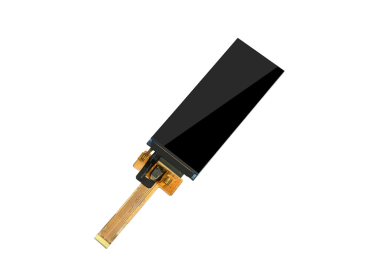
First, consider the entry points of electrostatic discharge (ESD) into the system. FPCs or board-to-board connectors pose a distinct system-level risk only if they are accessible to the user, located near coupling paths within the housing, or exposed during hot-swapping or maintenance. Fully enclosed, short-range direct connections on the board do not necessarily require additional ESD arrays.
A single D-PHY lane may have two electrical states.
Common implementations of forwarded-clock architectures utilize both data lanes and dedicated clock lanes, with the number of lanes employed by camera and display links varying according to system configuration. The signal lines themselves switch between high-speed differential signaling and low-power single-ended signaling. When ALP (Alternate Low Power) is enabled, the link can operate exclusively using high-speed signal levels, while embedded clock modes eliminate the need for a dedicated clock lane. Determining the specific implementation requires considering the host controller IP, the module, and the current configuration.
The D-PHY protection window must accommodate all line states associated with the current configuration. High-speed transmission is sensitive to additional capacitance and asymmetric parasitic effects, whereas low-power modes and power-up/power-down sequences require measures to prevent unintended device conduction. If issues such as unstable startup, display artifacts, or wake-up anomalies arise after the array is installed, the first step is to compare parameters such as junction capacitance (Cj), leakage current, and trace branching.
First, determine which locations require external protection.
Camera modules and mainboards are typically connected via FPC. Camera apertures, user-accessible areas, or adjacent metal structures can create paths for electrostatic coupling; protection placement must align with actual energy entry points, and both the mainboard and module sides should be evaluated.
Although display ribbon cables are not typically plugged or unplugged by users, they may route through hinges, metal brackets, or narrow housing sections. Determining the need for ESD protection requires looking beyond the "internal interface" classification to consider connector placement, housing gaps, cable routing, and the discharge path of the entire device.
During assembly and repair, reliance is primarily placed on production-line ESD controls; one should not add TVS diodes to high-speed lanes simply because the FPC might be touched during servicing. For direct chip-to-chip connections within enclosed areas, the decision to install protection components should be based on a combination of structural analysis and system-level testing. Even when reserving footprints for components, the layout must adhere to high-speed signal design principles, as the pads and branching traces themselves can introduce parasitic effects.
When consulting the parameter table, first check Cj, then verify the operating window and leakage.
First, verify the operating window. D-PHY signal levels—whether during high-speed operation, low-power modes, or power-up/power-down transitions—must remain within the device's permissible limits. Even for D-PHY interfaces, different host controllers, modules, and operating modes may require different protection voltage ratings.
When comparing junction capacitance (Cj), consider the test frequency and bias conditions; do not simply rely on the typical values listed on the datasheet's front page. Factors such as lane rate, trace length, connectors, FPC, vias, and receiver margin all influence the amount of additional capacitance the system can tolerate.
Differential pair mismatch is another concern. The Cj, pad configurations, and via environments for both lines should be as closely matched as possible; for multi-channel arrays, channel-to-channel variation must also be checked. A low nominal capacitance for a single channel does not guarantee that differential imbalance will not occur once the component is mounted on the PCB.
Clamping voltage and leakage current also require specific review. Clamping voltage must be coordinated with the transient withstand capability of the downstream port, while leakage current analysis must account for various temperature and power supply conditions—particularly scenarios involving independent module power, standby wake-up, or cases where one end is unpowered.
The array package must be aligned with the lanes.
While multi-channel arrays reduce component count, simply increasing the number of channels does not necessarily simplify the design. If the pinout is unsuitable, clock and data lanes may be forced to cross, change layers, or add branches. Although such arrays appear to save board space, the resulting routing and vias can actually introduce additional parasitic effects.
Array pin assignments should align as closely as possible with the FPC lane sequence: the signal path should flow from the connector into the array and then to the controller or module. If lane crossing or layer switching is required to accommodate the channel count, the package is likely unsuitable for the current board design. Ground pins should be connected to a ground plane with vias placed directly nearby.
The number of lanes indicates only how many lines require protection; it does not solely determine the specific model. When matching MIPI devices, ASIM also considers factors such as lane data rate, D-PHY mode, signal voltage levels (controller and module), FPC length, and connector placement.
The ESD protection for MIPI D-PHY should be laid out around the points of electrostatic entry.
For camera signal paths, protection points should be determined primarily based on apertures, accessible areas, and the entry points of FPCs onto the PCB; for display signal paths, potential energy entry points should be identified by considering bezels, hinges, and ribbon cable routing. Components should be placed close to actual entry points rather than simply following the location of the main control chip.
Component pads are part of the high-speed signal path. Abrupt widening of the gap between differential traces, significant changes in trace width or spacing, or the use of an unequal number of vias for the two traces can all create points of discontinuity. Ground connections should be short and direct to a continuous reference plane to minimize parasitic inductance in the discharge loop.
The connections between shielding cans, metal brackets, chassis ground, and digital ground must be handled consistently based on the overall system structure. Local ESD components can only limit voltage at specific protection nodes; they cannot replace proper chassis discharge paths or shielding connection designs.
Prototype validation must go beyond merely "producing drawings."
After installing the component, run the project at its maximum resolution and frame rate, and test cold/warm startups as well as standby-to-wake transitions. Additionally, vary the power-up sequence and conduct long-term operation tests to check for image flickering, signal drops, or initialization retries.
Where conditions permit, compare channel simulations, eye diagrams, or board-level signal measurements with and without the component installed. System-level ESD verification must also be performed separately, covering areas such as enclosure gaps, camera openings, display bezels, and the vicinity of connectors. In the event of a failure, troubleshoot the D-PHY link, module power supply, and control lines independently to avoid automatically attributing every "black screen" issue to the high-speed data lines.
Frequently Asked Questions
Can clock lanes and data lanes share the same type of ESD device?
In forwarded-clock mode, clock lanes and data lanes can share devices from the same series, provided that each channel meets the requirements for the actual operating window and junction capacitance (Cj). If pin assignments force a specific lane group to take a circuitous route, it is better to route them separately rather than forcing a shared package; in embedded-clock mode, the number of channels should be selected based on the actual lane configuration.
How low must the junction capacitance (Cj) be for D-PHY applications?
Do not start by setting a specific Cj value and then looking for a device. The acceptable range depends on factors such as lane rate, channel length, FPC characteristics, and receiver margin; after an initial selection, verification via simulation, eye diagrams, or functional stress testing is still required.
If the camera interface is located inside the housing, is ESD protection still required?
It depends on whether the ribbon cable and connector are close to apertures, metal brackets, or other coupling paths. For short-distance, direct connections within a fully enclosed space lacking obvious entry points, the decision can be based on structural assessment and system-level testing; however, interfaces located near camera apertures should not simply be treated as "internal connections."
Even though the component is close to the connector, why does the screen still go black during system-level testing?
Electrostatic discharge (ESD) can enter the system via the module's power supply, control lines, shielding structures, or reference ground. Issues such as excessively long ground loops, exposed traces prior to the protection circuitry, or a system controller reset can also manifest as a black screen. Troubleshooting should begin by determining whether the cause is a loss of D-PHY synchronization, a loss of power to the module, or a system reset.
 Previous

Related News
2026.07.13
How do I select a 5V low-capacitance ESD diode model?
2026.07.15
For what applications are SOD-323 packaged ESD diodes suitable?
2026.07.17
How should TVS diodes and common-mode inductors be configured for a CAN interface?
2026.07.17
How do you choose between SMA, SMB, and SMC packaged TVS diodes?
2026.07.20
How should a failure in the CAN communication surge test be handled?
2026.07.20
For which automotive applications is the SM8S series TVS suitable?
2026.07.20
How do you design a TVS protection solution for automotive power supplies?

2026.07.22
What issues need to be checked during EMC rectification?
2026.07.23
How do you implement ESD protection for USB Type-C interfaces? You need to select separate solutions for the data lines, CC lines, and VBUS.
2026.07.23
How to Design ESD Protection for HDMI Interfaces? Key Selection Criteria for TMDS High-Speed Lines and Control Lines


