





 Submit


What are the differences between SMA, SMB, and SMC packaged TVS diodes? Selection based on power and size.
 2026.07.24 00:00:00
 171
171





SMA, SMB, and SMC primarily refer to surface-mount package series rather than fixed power ratings. Based on common traditional TVS series (such as SMAJ, SMBJ, and SMCJ), the typical peak pulse power ratings for a 10/1000 μs pulse are 400 W, 600 W, and 1500 W, respectively, with the package sizes increasing in the same order. While this correspondence is useful for preliminary selection, it cannot replace the specific datasheets for individual part numbers.
When selecting a component, first determine the types of surges the power or signal lines will encounter, then consider the peak pulse current (IPP) and clamping voltage (VC) for the corresponding test waveform. While board space merely dictates whether the package fits, the downstream voltage withstand rating and surge current capability are what determine whether the component is actually suitable for use.
What exactly are the differences between SMA, SMB, and SMC?
The common JEDEC package designation for SMA is DO-214AC; among the three types, it occupies the least board space. It is suitable for power supply branches with low surge current requirements and limited PCB space, as well as for low-speed signal lines. While the common SMAJ series typically features a 400 W rating, products with higher or lower power ratings are also available in the same SMA form factor.
The SMB package corresponds to the DO-214AA standard; its package width and solder pads are generally larger than those of the SMA, and the common SMBJ series is rated at 600 W. In practical projects, a choice between SMA and SMB is frequently made for interface power supplies and the 24 V input branches of industrial control boards: the former saves space, while the latter offers greater margin for pulse current.
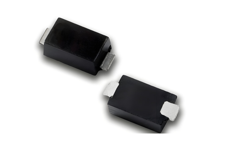
The SMC package corresponds to DO-214AB and features the largest physical dimensions and solder pads; the common SMCJ series is rated at 1500 W. It is better suited for power entry points characterized by low source impedance and high test currents. The trade-off is straightforward: the component itself, its solder pads, and the required surrounding clearance all consume more board space.
These power ratings must be accompanied by their test conditions. For the common, traditional series mentioned above—rated at 400 W, 600 W, and 1500 W—the peak power capabilities are specified based on defined temperatures, pad dimensions, and a 10/1000 μs pulse; other series may utilize different waveforms. These figures do not represent the power the device can dissipate continuously, nor can they be directly converted into surge handling capabilities for arbitrary pulse conditions.
Comparing package types for ASIM 24V-rated models.
When the voltage rating is held constant, the differences in packaging become more apparent. ASIM’s SMA04J24V, SMB06J24V, and SMC15J24V are all unidirectional TVS diodes; they all feature a VRWM of 24 V and a VBR range of 26.7–29.5 V. At their respective rated peak currents, all three exhibit a maximum VC of 38.9 V.
The primary difference lies in pulse capability. The SMA04J24V is rated at 400 W with an IPP of 10.3 A; the SMB06J24V at 600 W with an IPP of 15.5 A; and the SMC15J24V at 1500 W with an IPP of 38.6 A. These values must be applied in accordance with the specified pulse conditions and initial temperatures; one cannot disregard the waveform and assume the device can withstand the same current under any arbitrary surge condition.
This comparison demonstrates that the fact that all three devices share the same clamping voltage (VC) of 38.9 V does not imply identical performance. The VC values correspond to their respective peak pulse currents (IPP); if the application current is only 8 A, one should compare clamping performance in that range, whereas if the current reaches 20 A, the SMA and SMB packages fall outside their rated operating conditions.
The same series also includes the SMA04J24B, SMB06J24B, and SMC15J24B bidirectional versions. The choice between unidirectional and bidirectional types depends on the circuit's normal operating voltage range; replacements should not be selected based solely on package and power ratings for the sake of procurement convenience.
Do not determine power based on the package first.
The first item in the selection table should specify the surge test conditions. Since the durations of 8/20 μs and 10/1000 μs pulses, automotive pulses, and inductive turn-off spikes differ, the peak current a single TVS device can withstand varies accordingly. Simply comparing "600 W" and "1500 W" side-by-side makes it easy to overlook the differences in waveforms.
Next, consider the maximum normal operating voltage. The TVS diode's reverse standoff voltage (VRWM) must account for power supply tolerances, charging states, and steady-state upper limits; selection cannot be based solely on nominal values like 12 V or 24 V. Once the VRWM is determined, compare the breakdown voltage (VBR), the clamping voltage (VC) at the specified current, and the peak pulse current (IPP).
The VC value must be compared against the voltage ratings of the downstream MOSFET, power IC, and capacitors. A larger package does not necessarily imply a lower VC under all conditions; different series vary in terms of dynamic resistance, die size, and test current. When comparing two models, ensure that the waveform, IPP, and temperature are consistent across the comparison.
Under what circumstances should you upgrade from SMA to SMB or SMC?
If the IPP of an SMA device is already approaching its limit for the target waveform, or if the margin is insufficient after temperature derating, then SMB or SMC packages should be considered. This "upgrade" entails more than just switching to a larger solder pad; it requires re-verifying parameters such as VRWM, VC, leakage current, polarity, and the surge curve.
Another issue is that the downstream component's voltage withstand window is too narrow. Although a specific SMA-packaged model can handle the required current, the clamping voltage (Vc) under actual surge conditions exceeds the downstream component's tolerance; simply upgrading the package size is merely one potential option—identifying a specific series with suitable clamping characteristics is also essential.
Conversely, if the source itself possesses significant series impedance, the actual surge current is limited, meaning an SMC package may not yield tangible benefits. In such cases, using an SMA or SMB package—placing the device close to the input and shortening the discharge loop—is often a more rational approach than simply opting for a larger package size.
The PCB area is not limited to the footprint of the components themselves.
When examining the footprint, do not simply measure the dimensions of the molded package. You must also account for the distances involving solder pads, copper traces, and the path from the device to the return ground (including the path from the TVS itself). Just because the SMC body fits into the available space does not mean there is sufficient room around it to route a low-inductance discharge path.
Pulse capability ratings in datasheets are typically based on specific solder pad or copper area dimensions. If pads are reduced to save board space in a prototype, or if a long, thin trace is used to connect the TVS to a distant ground plane, the actual temperature rise and residual voltage will deviate from the datasheet specifications. Furthermore, in high-temperature environments, you must re-evaluate the design using derating curves rather than relying on ratings specified for 25°C.
When selecting a TVS device, you should first determine the target waveform, maximum surge current, and the voltage withstand rating of the downstream circuitry before considering SMA, SMB, or SMC packages. Only after verifying these parameters can you determine whether a larger package is actually required.
What is most easily overlooked when substituting part numbers?
Even among SMA, SMB, or SMC packages, pad dimensions, component heights, and polarity markings are not necessarily identical. Suffix conventions vary by manufacturer; one should not rely on guesswork to distinguish between types such as A, CA, unidirectional, and bidirectional. Before substitution, verify the package outline, recommended pad layout, internal structure, and silkscreen orientation.
Identical VRWM ratings do not guarantee identical electrical performance. Factors such as the VBR range, the test current corresponding to VC, leakage current, and the temperature coefficient all influence the outcome. When sourcing a substitute, simply specifying "SMBJ24 with the same package and voltage" is insufficient; the target test conditions and the voltage withstand rating of the downstream circuitry must also be included.
Common Issues with SMA, SMB, and SMC Packages
Can a 600 W SMB device directly replace a 400 W SMA device?
No, they are not directly interchangeable. The two packages have different pad layouts, and parameters such as VRWM, VC, IPP, polarity, and component height must be re-verified. Even if the PCB layout can be modified, the 600 W rating applies only under specified waveform and temperature conditions.
Does a larger package (like SMC) necessarily result in a lower clamping voltage?
Not necessarily. Clamping voltage (VC) depends on the specific chip structure, dynamic resistance, and pulse current. Specific part numbers should be compared under identical waveform, current, and temperature conditions; comparing package sizes alone is insufficient.
The datasheet specifies 1,500 W; can it withstand 1,500 W of continuous power?
No. The PPPM rating of a TVS diode refers to its short-duration pulse capability; specifications typically also define the waveform, initial junction temperature, and repetition rate. Handling continuous overvoltage requires the use of fuses, current limiting, electronic circuit breakers, or other power protection circuitry.
If the surge current is unknown, can you initially allocate space for an SMC package?
You can use this approach for the prototype stage, but you shouldn't finalize the design based on it. First, check the testing standards, open-circuit voltage, source impedance, and pulse waveform, then estimate the current through the TVS branch. Without clear parameters, simply choosing a larger package cannot guarantee effective protection.
Before submitting your package selection, compile a table listing the maximum normal operating voltage, surge waveform, peak current, downstream voltage tolerance, ambient temperature, and available pad area. Review each item carefully before deciding whether to use SMA, SMB, or SMC.
 Previous

Related News

2024.10.12
EMC testing Contents and Current Situation of Automotive Electronic products

2025.02.21
How to choose the best circuit protection devices in a circuit?
2026.07.13
How do I select a 5V low-capacitance ESD diode model?
2026.07.16
How do I select the package for a TVS diode used with a 24V power supply?
2026.07.17
How do you choose between SMA, SMB, and SMC packaged TVS diodes?
2026.07.20
How should a failure in the CAN communication surge test be handled?
2026.07.20
How do you design a TVS protection solution for automotive power supplies?

2026.07.22
What issues need to be checked during EMC rectification?
2026.07.23
How do you implement ESD protection for USB Type-C interfaces? You need to select separate solutions for the data lines, CC lines, and VBUS.
2026.07.23
How to Select Low-Capacitance ESD Protection for MIPI D-PHY Interfaces: Key Design Considerations for Camera and Display Links


