





 Submit


ESD protection for the gate of SiC/GaN power devices: Why it is more difficult to protect than IGBT
 2026.06.10 00:00:00
 197
197





In 2026, silicon carbide (SiC) and gallium nitride (GaN) power devices are at the critical point of transitioning from technological validation to large-scale mass production - 800V electric vehicle main drive inverters, photovoltaic inverters, and GaN fast charging adapters are widely adopting these two types of devices. However, a key characteristic of SiC/GaN that is often overlooked is that their gate is much more fragile than that of IGBT, with a thinner gate oxide layer, lower withstand voltage, and greater sensitivity to ESD. Applying the traditional IGBT gate protection scheme directly to SiC/GaN will leave hidden risks. This article clarifies the special requirements and design methods for SiC/GaN gate ESD protection.
The key differences between SiC/GaN gate and IGBT gate
| Comparison Dimension | IGBT | SiC MOSFET | GaN HEMT |
|---|---|---|---|
| Gate Oxide Layer Thickness | Thicker (>50nm) | Thinner (~40nm) | GaN without Oxide Layer (Schottky Gate) |
| Recommended Gate Voltage | +15V/−8V | +20V/−5V (Typical) | +5V/−3V (Typical) |
| Gate Maximum Voltage (Vgs max) | ±20V | ±25V | ±10V (Lower) |
| Gate ESD Tolerance (HBM) | Usually 1kV~2kV | About 500V~1kV | About 100V~500V (Extremely Low) |
| Negative Voltage Requirement During Turn-off | Partly Required | Required (To Prevent Mis-triggering) | Mostly Required |
Key conclusion: The gate ESD tolerance of GaN HEMT is only 100 to 500V, which is much lower than the 2kV or above of IGBT. When handling GaN devices, human static electricity (typically 2kV to 8kV) could easily break through the gate, but you won't even notice any abnormality.
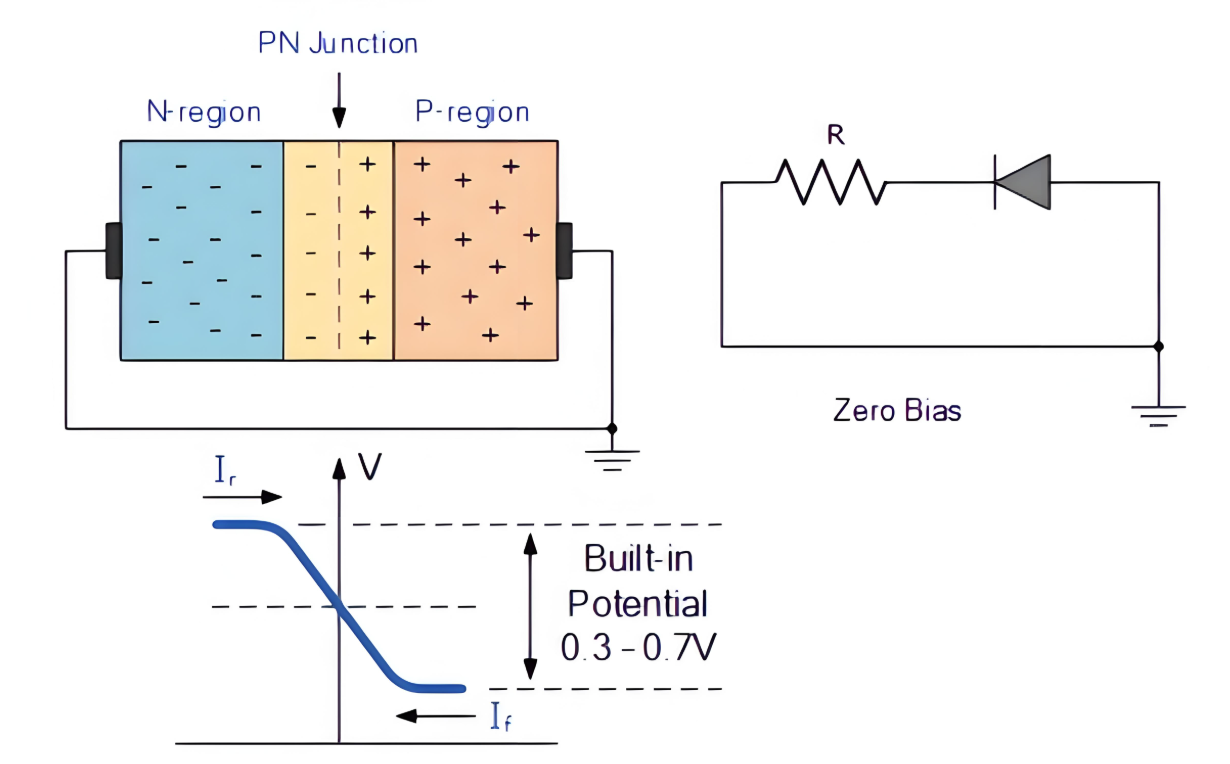
SiC Gate Protection Scheme
Typical gate operating parameters of SiC MOSFET:
Operating voltage: +15V to +20V
Shutdown voltage: -5V to 0V (negative voltage shutdown to prevent accidental triggering)
Vgs max: ±25V (for most SiC products)
Gate TVS selection (critical)
The SiC gate TVS must meet the following requirements:
VRWM ≥ The highest open voltage (+20V), and at the same time, the reverse VRWM ≥ The absolute value of the highest negative pressure (5V)
Bidirectional TVS: Overvoltage transients may occur during both turn-on and turn-off processes.
The capacitance of the junction capacitor (Cj) should be low: The gate circuit is a high-impedance circuit, and parasitic capacitance can affect the switching speed.
Asim's recommended model (bidirectional TVS for SiC gate):
| Model | VRWM | VC(max) | Polarity | Package | Applicable |
|---|---|---|---|---|---|
| SMBJ20CA | 20V | 32.4V | Bidirectional | SMB | SiC 20V switching system |
| SMAJ20CA | 20V | 32.4V | Bidirectional | SMA | Space-saving scenarios |
| SMBJ18CA | 18V | 29.2V | Bidirectional | SMB | Low clamping voltage requirement |
Selection criteria: The clamp voltage VC must be lower than Vgs max (25V). Otherwise, the gate will be broken down first and then clamped by the TVS diode, which is too late.
Gate protection circuit
Driver IC output ↓ Gate resistor Rg (typically 5-20Ω, for controlling dv/dt) ↓ [SMAJ20CA bidirectional TVS] (clamping gate overvoltage) ↓ SiC MOSFET gate (Gate) | [10-47Ω pull-down resistor] (preventing floating mis-triggering) | Source (reference ground) ### ESD protection for driver IC output
The output pins of the driver IC (PWM input, Fault output) will be subjected to electrical impulse during the system-level ESD test:
Control board PWM signal ↓ [DFN1006-2L bidirectional ESD (VRWM = 5V)] ↓ Input pins of the driver IC ## GaN HEMT gate protection scheme
The gate of GaN devices is more fragile and requires stricter protection.
Typical gate parameters of GaN HEMT (taking 650V GaN as an example):
Operating voltage: +5V (E-mode enhanced version)
Shutdown voltage: 0V or -3V
Vgs max: ±7V to ±10V (minimum)
Gate ESD tolerance: 100 - 500V (extremely low, with almost no margin)
Selection of GaN Gate TVS
The Vgs max of GaN is only ±7V to ±10V, so the clamping voltage must be controlled within this range:
| Parameter | Value |
|---|---|
| TVS VRWM | 5V (matching turn-on voltage) |
| TVS VC(max) | <8V (lower than Vgs max by 10V) |
| Polarity | Bidirectional |
This means that the clamp voltage range is extremely narrow (5V to 8V), and most standard TVS devices on the market do not meet this requirement - special low-clamp TVS or TVS + zener diode combinations are needed.
It is recommended to confirm the specific model with the Assem technical team, provide the GaN model and Vgs max parameters, and the technical team will offer the optimal clamping solution.
ESD Protection for GaN Devices During Assembly
The ESD protection requirements during the assembly stage of GaN devices are much stricter than those for IGBTs:
The operation must be carried out in a well-structured ESD protection work area (EPA).
Operators must wear grounding wrist straps (with resistance less than 1MΩ)
The workbench must be covered with an anti-static mat.
After removing the GaN device from the packaging, insert it directly onto the circuit board immediately. Do not leave it exposed for a long time.
Immediately short-circuit the gate to the Source after welding (to prevent static electricity accumulation after welding)
Five Common Mistakes in SiC/GaN Gate Protection
Error 1: Using the protection scheme of IGBT directly with a gate withstand voltage of ±20V for IGBT. Common TVS diodes are usually selected as 24V unidirectional. This is completely inappropriate for SiC/GaN - the voltage range and polarity may be incorrect.
Error 2: Ignoring the protection of negative pressure shutdown. Most SiC devices use negative pressure (−5V) for shutdown, and a negative voltage overshoot may occur during the shutdown moment. Bidirectional TVS diodes must be used; they cannot be used only for protection of the positive side.
Error 3: Excessive capacitance of TVS diode. The gate circuit has high impedance. A large capacitance TVS diode will increase the switching rise/fall time, affecting the switching efficiency. For SiC/GaN gate TVS diodes, select models with a capacitance of less than 50pF.
Error 4: The TVS is too far from the gate pin. The longer the trace from the gate to the TVS, the greater the equivalent parasitic inductance, and the slower the protection speed. The TVS must be close to the gate pin (with the trace < 5mm), and the GND loop should be the shortest.
Error 5: During assembly, without proper EPA protection, operating the GaN GaN gate with an ESD tolerance of 100 to 500V leaves almost no margin. Even if the electrostatic accumulation in the working area is not significant (within 200V), it can still cause hidden damage to the gate - the device can still switch normally, but the oxide layer is partially damaged, and the lifespan is significantly shortened.
Common Questions and Answers about SiC/GaN Gate Protection
Q: After SiC devices have been operating in the frequency converter for a period of time, their efficiency decreases. Could it be that the gate has been damaged?
A: Possibly. Progressive damage to the gate oxide layer (accumulated impact from multiple ESD events) can cause the threshold voltage Vth to drift, thereby affecting the switching characteristics - manifested as an increase in switching time, rise in loss, and decrease in system efficiency. Diagnostic method: Use an oscilloscope to measure the gate waveform, check if there are any abnormal peaks in Vgs; compare the current Vth with the initial specification value to see if there is any deviation.
Q: The GaN fast charging adapter keeps breaking frequently. Could it be that the gate has been damaged by ESD?
A: Static electricity generated when the user plugs or unplugs the charger may be conducted through the power line to the gate of the GaN device. Due to the extremely low tolerance of the GaN gate, even if a TVS is installed, if the clamping voltage of the TVS is too high or the response speed is insufficient, it may still cause latent damage. Rectification direction: ① Check if the clamping voltage of the TVS for the GaN gate in the driving circuit is less than Vgs max; ② Strengthen ESD protection at the power line inlet (using a MOV + TVS combination); ③ Confirm that the EPA protection during assembly is in place.
Q: Can Asim provide a gate protection solution for SiC/GaN power devices?
A: Yes. The Assem TVS product line covers ±20V bidirectional low-clamping TVS (SMBJ20CA series) required for SiC gate protection. For the ±5V ultra-low-clamping TVS solution for GaN gates, you can contact the Assem technical team for customized consultation. Contact number: 400-014-4913 / 18822897174 (same number for WeChat).
Regarding Asim (ASIM): Asim was established in 2013 and is a professional ESD/TVS protection device manufacturer located in Shenzhen. It produces over 1200 types of TVS diodes, covering bidirectional low clamping TVS required for SiC/GaN gate protection. It also provides EMC laboratory services for system-level ESD testing and rectification for SiC/GaN systems. National consultation hotline: 400-014-4913

 Previous

Related News

2024.10.12
EMC testing Contents and Current Situation of Automotive Electronic products

2025.02.21
How to choose the best circuit protection devices in a circuit?
2025.08.25
TVS diodes solve the problem of WIFI disconnection in routers due to ESD interference-ASIM

2025.08.26
ESD electrostatic protection failure? It might be that you have chosen the wrong ESD diode! -ASIM
2025.09.04
How to correctly apply polymer ESD in high-speed interfaces? -ASIM
2025.09.09
Analysis of Misunderstandings in TVS Tube Clamping Voltage Selection and Calculation -ASIM
2025.09.10
The Function and Working Principle of MOSFETs -ASIM

2025.11.17
What is an eye diagram? A comprehensive guide to the function and principle of eye diagrams - ASIM Electronics
2025.12.18
ESD Diode Failure Analysis: Surge Tolerance and Short Circuit Risk-ASIM
2026.05.19
What Is an ESD Diode? Working Principle, Key Parameters & Selection Guide


