





 Submit


What should be done if signal abnormalities occur after adding ESD protection to a MIPI interface?
 2026.07.15 00:00:00
 80
80





Signal anomalies occurring after the addition of ESD protection to a MIPI interface are typically associated with excessive ESD junction capacitance, high package parasitic parameters, overly long layout branches, asymmetry in differential lines, or discontinuities in the reference ground. Remediation efforts should address both device parameters and PCB layout, rather than focusing solely on whether the ESD device itself provides adequate electrostatic protection.
I. Common Anomalies
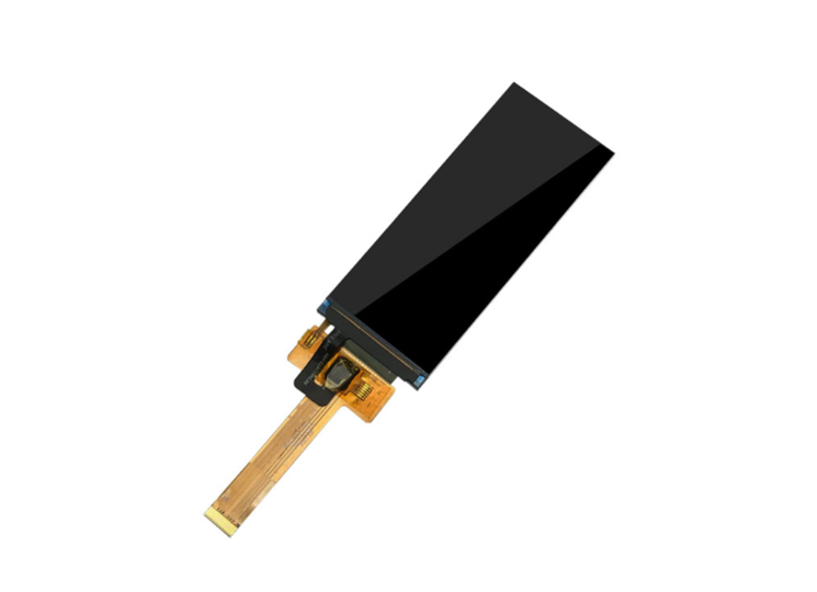
Anomalies in the MIPI interface may manifest as the camera failing to be recognized, screen artifacts (garbled display), image flickering, reduced frame rates, intermittent black screens, or degraded EMI performance. If issues arise only after adding ESD protection, signal integrity should be the first area investigated.
If the system passes electrostatic discharge (ESD) testing but exhibits functional instability, it suggests that the protection components may be interfering with the high-speed link.
II. Key Factors
The primary factors are: excessive ESD junction capacitance altering the differential line load; additional parasitic effects introduced by device packaging and pads; excessively long branches extending from the main signal lines; asymmetry between the left and right channels; and issues with the reference ground plane, such as slotting or an insufficient number of vias.
Higher MIPI data rates increase sensitivity to these factors; layout practices acceptable for low-speed interfaces may not be suitable for MIPI.
III. Remediation Methods
Replace with ESD components featuring low junction capacitance and low-parasitic packaging; place components close to the connector and shorten branch traces; maintain differential pair symmetry; ensure a complete reference ground plane; and re-evaluate impedance and eye diagrams if necessary.
Following remediation, verify image stability, ESD test results, and critical high-speed signal waveforms.
IV. Asym Support
Asym provides recommendations for selecting low-capacitance ESD protection devices for MIPI interfaces and offers guidance on EMC testing and remediation, helping customers strike a balance between electrostatic protection and signal integrity.
FAQ
Q: Does a scrambled screen on a MIPI interface after adding ESD protection indicate a defective component?
A: Not necessarily; issues often stem from junction capacitance, component placement, or impedance continuity.
Q: Does reducing ESD capacitance compromise protection performance?
A: A balance must be struck between low capacitance and clamping capability; one cannot rely on a single parameter alone.
Q: Is a PCB review necessary when troubleshooting ESD issues on a MIPI interface?
A: Yes. High-speed interface issues are frequently closely linked to component placement and trace routing.
 Previous

Related News

2024.10.12
EMC testing Contents and Current Situation of Automotive Electronic products
2025.09.08
High-frequency Circuit TVS Diode Junction Capacitance Optimization Strategy -ASIM
2025.09.09
Analysis of Misunderstandings in TVS Tube Clamping Voltage Selection and Calculation -ASIM
2025.09.12
How to effectively dissipate heat and solve the problem of severe heating of MOSFETs? - Shenzhen ASIM
2025.12.18
ESD Diode Failure Analysis: Surge Tolerance and Short Circuit Risk-ASIM
2026.06.22
TVS Diode VRWM, VBR, and VC: Parameter Relationship Guide
2026.06.22
ESD Diode vs TVS Diode: Which to Use and When
2026.07.10
What is the difference between automotive-grade TVS and standard TVS?
2026.07.11
How is the ESD0524 series used for USB interfaces?
2026.07.11
How do you design an ESD protection scheme for USB interfaces?


