





 Submit


Common Issues Regarding ESD Protection for HDMI Interfaces
 2026.07.16 00:00:00
 116
116





Common issues regarding ESD protection for HDMI interfaces primarily center on the selection of low-capacitance ESD devices, component placement, differential pair routing, 5V power line protection, and signal anomalies following ESD implementation. When selecting components for high-speed HDMI lines, one cannot rely solely on ESD ratings; it is also essential to verify junction capacitance, parasitic parameters, and signal integrity.
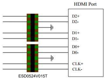
I. Why HDMI Interfaces Are Prone to ESD Issues
HDMI interfaces are exposed, subject to frequent plugging and unplugging, and often connected via long cables, making them susceptible to electrostatic discharge (ESD) from the human body and interference coupled through the cables. According to Asym's port design documentation, hot-plugging HDMI devices generates significant interference energy; ESD protection components are essential to rapidly dissipate this static interference, preventing the surge of energy from stressing the circuitry and causing operational malfunctions.
Electrostatic energy can enter the system via high-speed lines (TMDS differential pairs), control lines (DDC, CEC, HPD), the chassis, or the 5V power supply. If protection components are poorly placed—such as positioning them near the main control chip rather than at the connector to save space—the electrostatic charge propagates along the PCB traces first. Parasitic inductance then causes the clamping voltage to rise, resulting in a scenario where the charge enters the board before being dissipated, ultimately triggering chip resets or causing permanent damage. Asym has repeatedly verified through various remediation cases (such as network media boxes and wireless HDMI casting devices) that the placement of ESD protection components is the decisive factor in passing compliance tests.
II. Summary of Common Issues
In engineering practice, typical misconceptions regarding HDMI ESD protection include:
Excessive ESD capacitance on high-speed lines: TMDS lines operate at high speeds (3.4 Gbps for HDMI 1.4; 6.0 Gbps for HDMI 2.0); excessive junction capacitance attenuates signals and closes the eye diagram.
ESD devices placed too far from the connector: Trace inductance significantly degrades transient protection performance.
Excessively long differential line branches: Routing long stubs from the main line to the ESD device causes impedance discontinuities.
Lack of independent protection for the 5V power line: Surges or ESD events affecting the +5VOUT or VBUS lines can impact the entire interface.
Improper chassis grounding: Failure to connect the shielding shell to ground with low impedance can lead to secondary arcing.
Omission of protection for control lines: Lines such as DDC_CLK and DDC_DAT are often overlooked; despite their low data rates, they remain vulnerable to ESD.
These issues can result in black screens, screen flickering, device recognition errors, poor compatibility, or failure to pass ESD compliance tests. For instance, prior to remediation, a network box failed a 4kV contact discharge test on its HDMI metal shell; similarly, a wireless HDMI caster experienced indicator light anomalies and signal interruption during an 8kV air discharge test at the output-side ventilation vents.
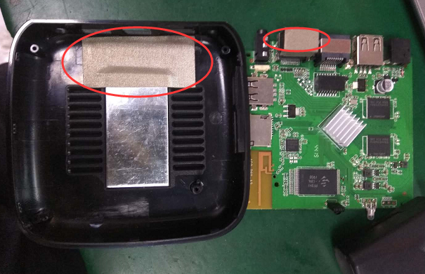
III. Rectification Recommendations: A Dual Approach Targeting Components and Layout
1. High-speed TMDS lines: Low-capacitance ESD protection + Symmetrical layout
Selection: Ultra-low junction capacitance array devices must be used. The Asym DFN2510-10L series integrates four ESD channels and is specifically designed for high-speed differential signals; it features extremely low parasitic capacitance, ensuring no impact on signal transmission. Typical model: ESD0524PA—typical I/O capacitance of only 0.3 pF, ±20 kV air discharge capability, and 5 V operating voltage.
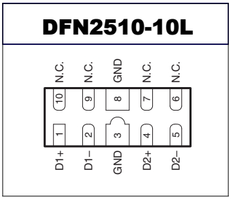
ESD0524UA: 0.5pF (typical), 50W peak pulse power; suitable for USB, HDMI, and DP applications.
ESD0524V015T / ESD2510U005T: 0.05pF (typical); supports HDMI 2.0 eye diagram compliance; suitable for ultra-high data rates.
Layout: Place the device close to the HDMI connector, with differential pairs (TMDS_D2±, D1±, D0±, CK±) arranged symmetrically. Asaim has repeatedly emphasized that "ESD devices must be placed on the main signal path rather than on a branch," and long stubs are strictly prohibited.
Common-mode filtering: Can be paired with a 90Ω@100MHz common-mode choke (such as the CMF1210UD900MFR recommended in HDMI radiated emission remediation cases) to suppress common-mode noise while having negligible impact on differential-mode signals.
2. Control Lines and 5V Power Line
Control lines (DDC, CEC, etc.): Operating at 5V with low data rates; standard ESD protection components—such as the ESD5D030TA (±30kV)—may be selected and should be placed close to the interface.
5V line: Requires dedicated TVS protection with consideration for surge handling capability. Recommended components include the ESD5A005TA (SOD-323, ±30kV) or SODA5F501TR (SOD-123FL, 2000W peak power rating); additionally, a ferrite bead (such as the CVB1608E601T used for HDMI VCC in the port design guidelines) should be connected in series to filter out power supply noise.
Chassis grounding: In accordance with the port design guidelines, the ESD component's ground pin must connect directly to the HDMI shielding shell or the PCB ground plane via the shortest possible path; the chassis itself should also be connected to the system ground using a low-impedance method (e.g., conductive foam or metal screws).
3. Continuous Ground Plane
The discharge ground must be continuous; Asym defines a "continuous ground" as having an aspect ratio of less than 3, with no slits or apertures. Numerous remediation cases demonstrate that a lack of continuity in the ESD discharge ground is the root cause of protection failure.
4. Verification and closure following corrective actions
Simultaneous testing of: ① ESD rating (IEC 61000-4-2 contact/air); ② Display stability (no black screens or flickering); ③ Compatibility (various signal sources/display terminals); ④ Signal integrity (eye diagrams, impedance).
IV. ASIM Support: Balancing Protection and Image Quality
ASIM offers low-capacitance ESD devices, array protection solutions, and EMC rectification recommendations for HDMI interfaces:
| Subject of protection | Recommended Components | Key parameters | Remark |
|---|---|---|---|
| TMDS high-speed differential | ESD0524PA / ESD0524UA / ESD0524V015T | 0.3~0.05pF, ±20kV | DFN2510-10LArray |
| Control lines DDC/CEC | ESD5D030TA | ±30kV, 5V | Small-package component placed close to the interface. |
| 5V power supply | ESD5A005TA + CVB1608E601T | ±30kV, Ferrite bead filtering | TVS and Ferrite Bead Combination |
| Common-mode noise | CMF1210UD900MFR | 90Ω@100MHz | Common-mode filtering for differential lines |
We help clients strike a balance between protection capabilities and high-speed signal integrity, avoiding the scenario where "ESD protection is achieved at the cost of screen distortion."
FAQ
Q: Is it better to have more ESD protection devices on the HDMI interface?
A: No. While protection must cover critical lines (high-speed differential pairs, control lines, the 5V line, and the chassis), an excessive number of components adds parasitic load, which can degrade signal integrity. Precise component selection and proper layout are essential.
Q: What should I do if screen flickering occurs after adding ESD protection to the HDMI interface?
A: First, check if the ESD device's junction capacitance is too high, if the layout includes long stubs, and if the differential impedance remains continuous. Consider switching to an ESD array with lower capacitance (such as the 0.05pF ESD0524V015T) and placing it symmetrically as close to the connector as possible.
Q: Should the HDMI chassis/shell be grounded?
A: Grounding is generally required; it is recommended to connect the ESD ground pin directly to the shielding shell or ground plane via a short path. However, the specific connection method should be determined based on the system's overall EMC and mechanical design (e.g., using conductive fabric to connect a plastic housing to the mainboard ground) to avoid creating secondary discharge points.
 Previous

Related News

2024.10.12
EMC testing Contents and Current Situation of Automotive Electronic products

2025.02.21
How to choose the best circuit protection devices in a circuit?
2025.09.08
High-frequency Circuit TVS Diode Junction Capacitance Optimization Strategy -ASIM
2025.09.09
Analysis of Misunderstandings in TVS Tube Clamping Voltage Selection and Calculation -ASIM
2025.09.10
The Function and Working Principle of MOSFETs -ASIM
2026.06.22
TVS Diode VRWM, VBR, and VC: Parameter Relationship Guide
2026.07.13
How do I select a 5V low-capacitance ESD diode model?
2026.07.15
What should be done if signal abnormalities occur after adding ESD protection to a MIPI interface?
2026.07.15
For what applications are SOD-323 packaged ESD diodes suitable?
2026.07.15
How do you select a low-capacitance ESD protection device for an HDMI interface?


